The LasNova 50 is a 532nm (green) DPSS laser capable of a maximum of 100mW of output power. The LasNova series produce a very high quality, Gaussian beam, and have quite a narrow bandwidth. This particular LasNova 50 has an interesting history. It was generously donated to us by Patrick, but is not in working condition. This is because this laser head, along with multiple others, has been subjected to what Patrick describes as "radical decommissioning". Essentially, when the piece of OEM equipment was being decommissioned and parted out, the laser head was subjected to several direct strikes from a screwdriver. The damage caused by this varies between the units that Patrick received, but we got one of the worst ones (no complaints though, as it was free!). Regarding the reasoning for this episode of "radical decommissioning", we have two theories:
1. The individual disassembling the equipment was suddenly enraged due to an unknown circumstance and decided to unleash their wrath on the laser heads
2. During the decommissioning process, the laser heads were intentionally damaged to prevent re-use, likely for compliance or safety reasons
We'll go with option 2, as that is probably what happened. We have seen this happen to other electronic devices as well, usually it takes the form of cut cables or connectors, which also prevent re-use of the device. While this is incredibly wasteful, it is more common than you would expect. It is often done for compliance reasons, especially with equipment such as lasers that can be dangerous if misused. While we do not agree with this practice, we do understand why it is done.
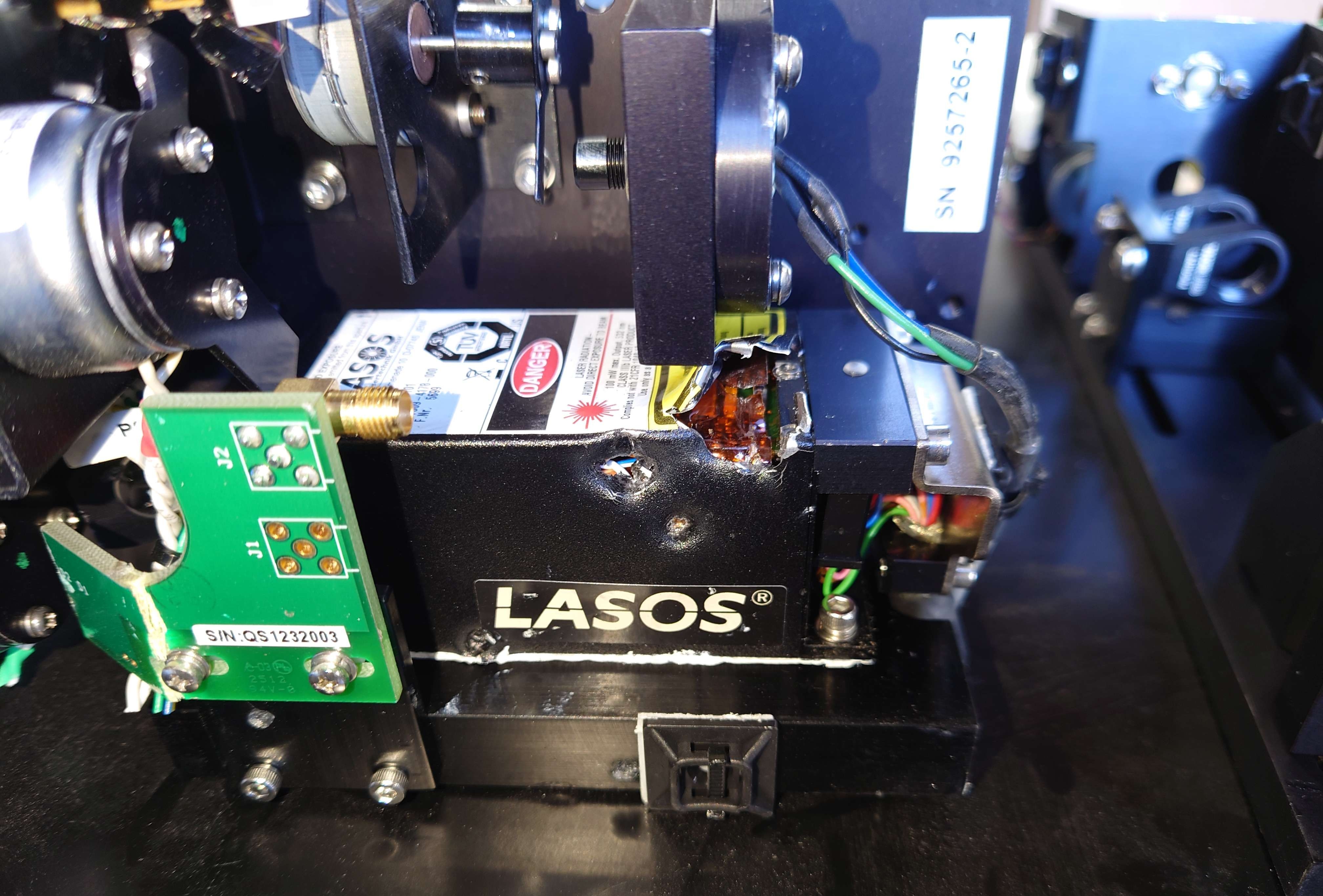
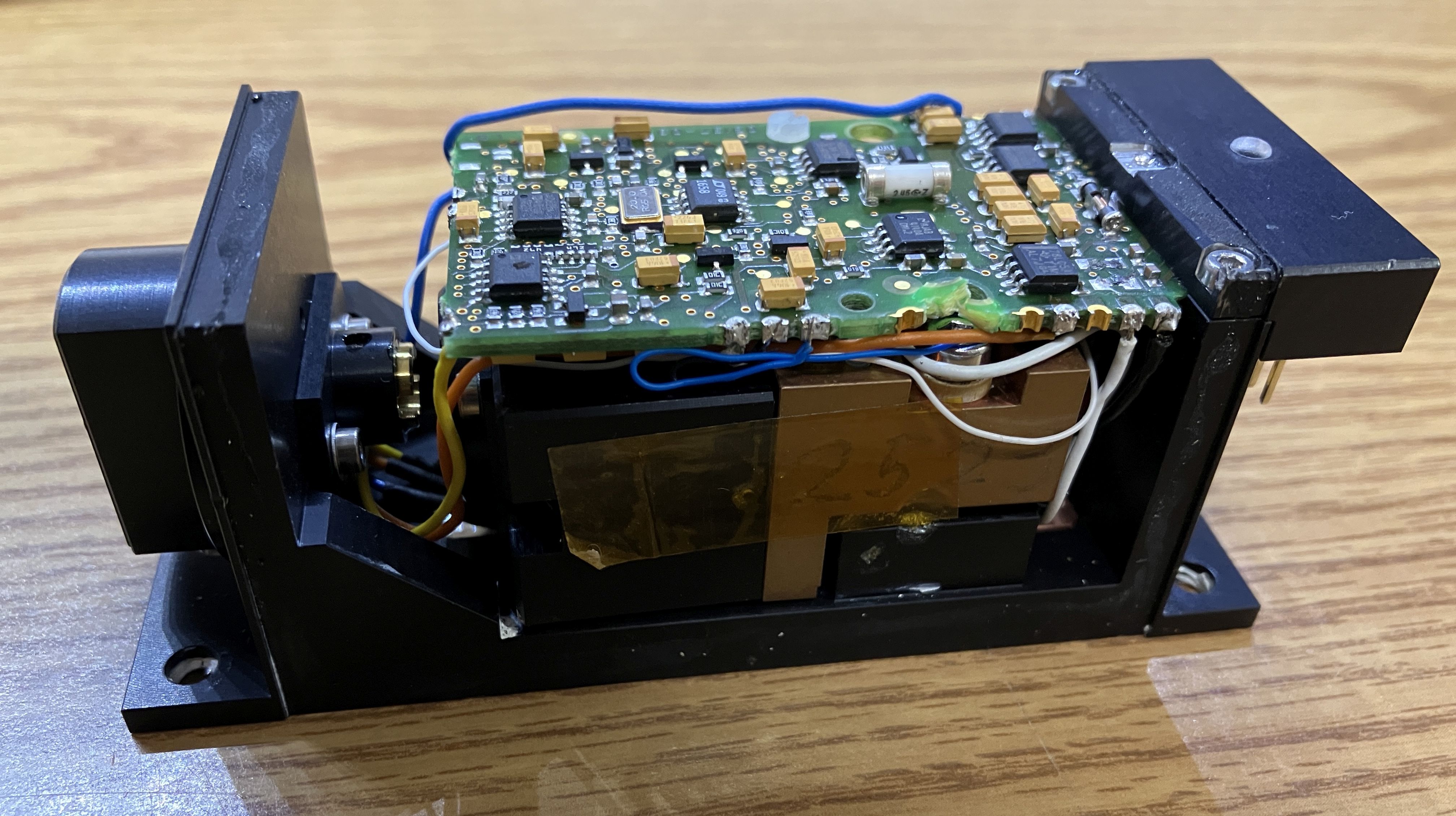
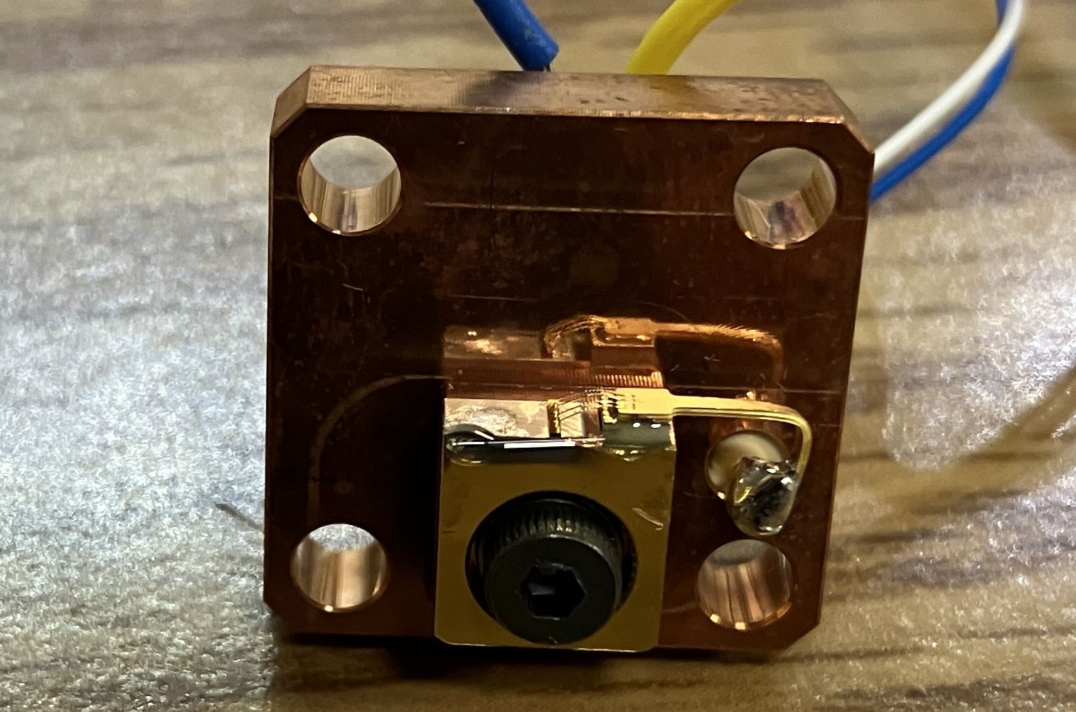
Opening the case for the first time is a bit challenging as while there is only one screw on the top (near the LED), there is glue all around of the perimeter of the casing. This must be separated carefully to remove the thin aluminum cover without bending or damaging it. Once removed we can see the inside of the laser head. The circuit board is mounted on top via some (broken) nylon screws and two metal screws on the back metal portion near the LED. The circuit board and the back metal portion are bonded together as this is where the pin header connector is mounted. The optical cavity and components sit below the board and attach to the bottom of the case.
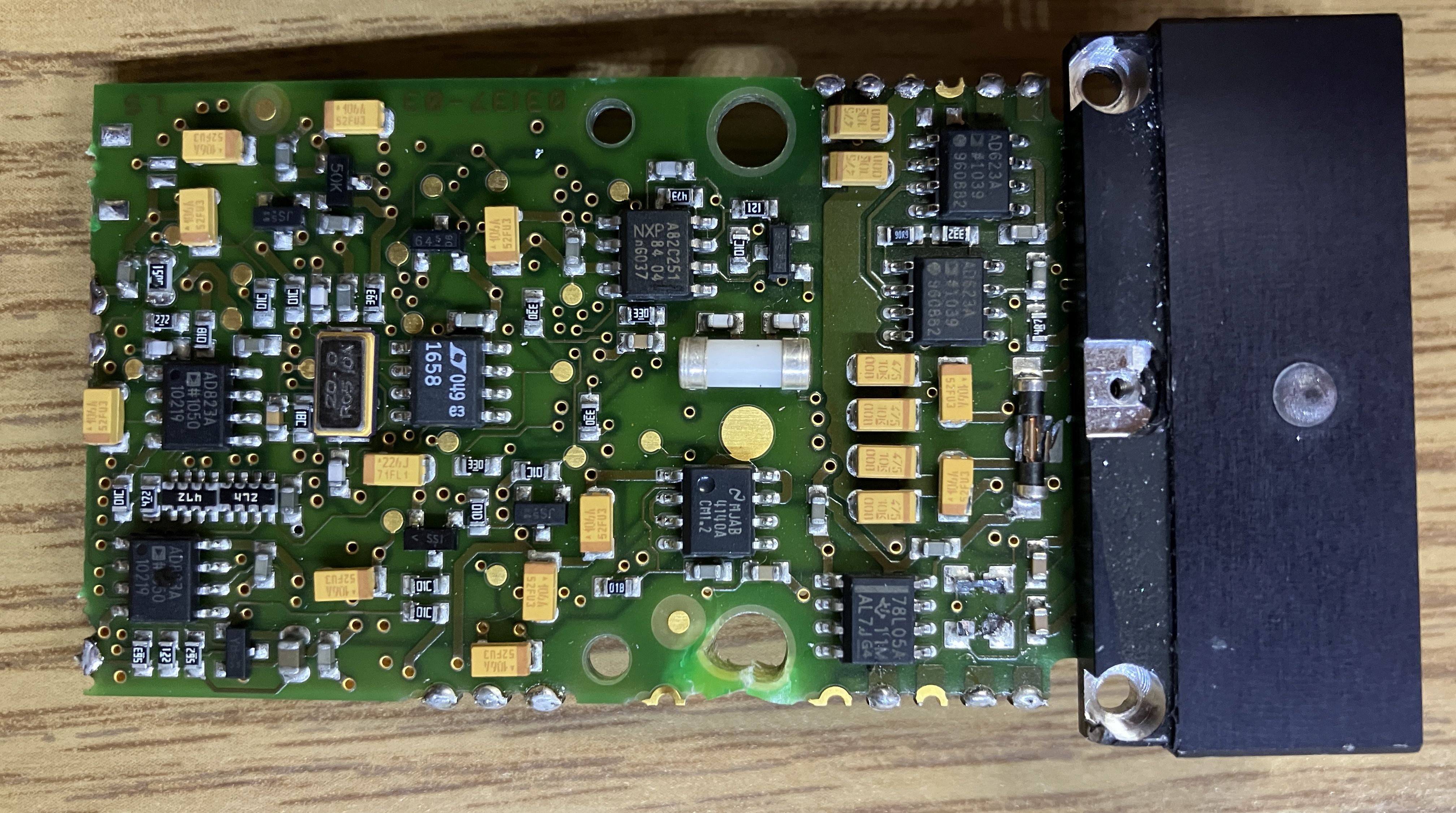
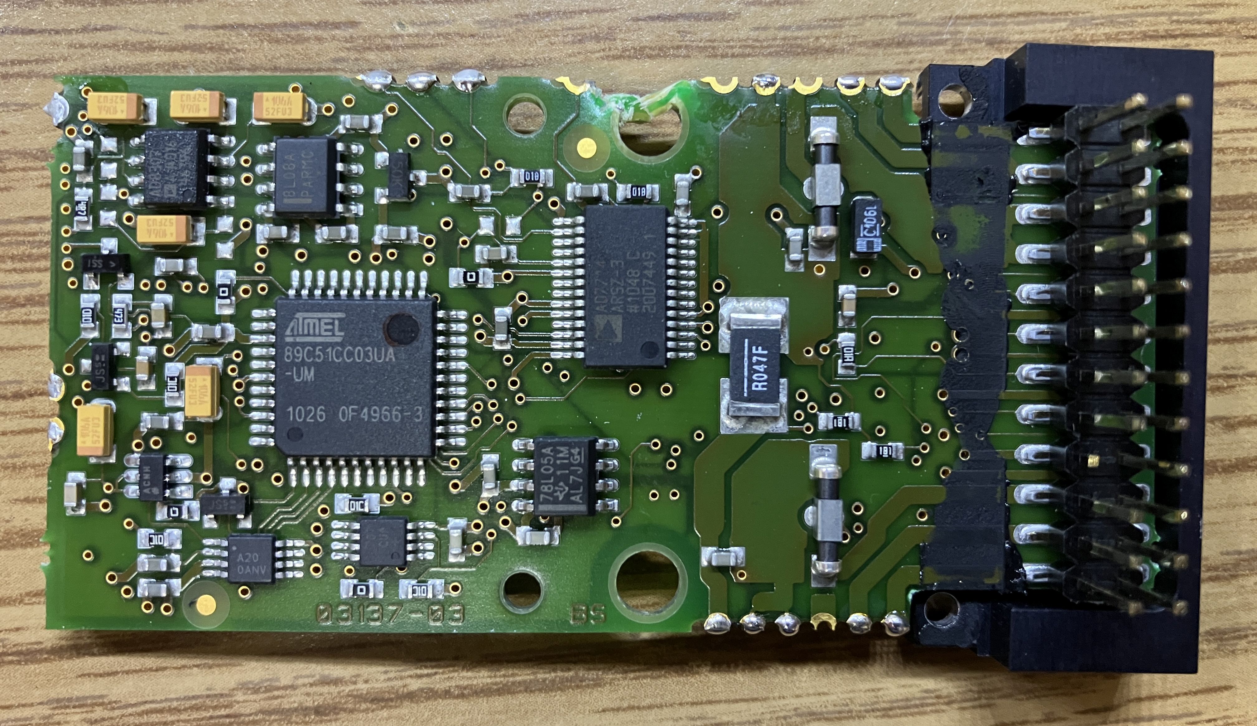
On the top side of the circuit board, most of the damage sustained was directly on a hole within the side of the PCB, which is probably the best possible outcome. The only damaged component that we found on this board is on the rightmost side near the center of the board. We are unsure of the purpose of this component (perhaps a fuse or resistor), but it is clearly damaged. The LED is also visible on the right side metal bracket that is attached to the PCB. Notable components on this side include several surface-mount capacitors, a crystal oscillator, and multiple Analog Devices amplifiers. Additionally, the NXP A82C251 is a CANbus transceiver, which is interesting. Perhaps this laser head uses CANbus to communicate with the OEM driver board.
On the bottom side of the circuit board, we can see the pin header for the cable that connects to the driver board as well as some more digital components. The ATMEL chip is an 8-bit MCU with CAN support and some built-in flash memory. This is clearly the primary processor for the functions controlled within the laser head. As mentioned earlier, it probably communicates with the OEM driver board over CANbus. The large component from Analog Devices is an analog-to-digital converter. Wires from the components within the laser head such as TECs, temperature sensors, and the pump diode, all connect to this board using side-mounted solder connections. This is relatively uncommon, but actually makes removing the board easier as the solder connections (gold semi-circles on side of PCB) are easily accessible on both sides of the board when installed in the laser head.
With the circuit board removed, we can see two individual housings joined together at the center, as well as the wires that connect to the board.
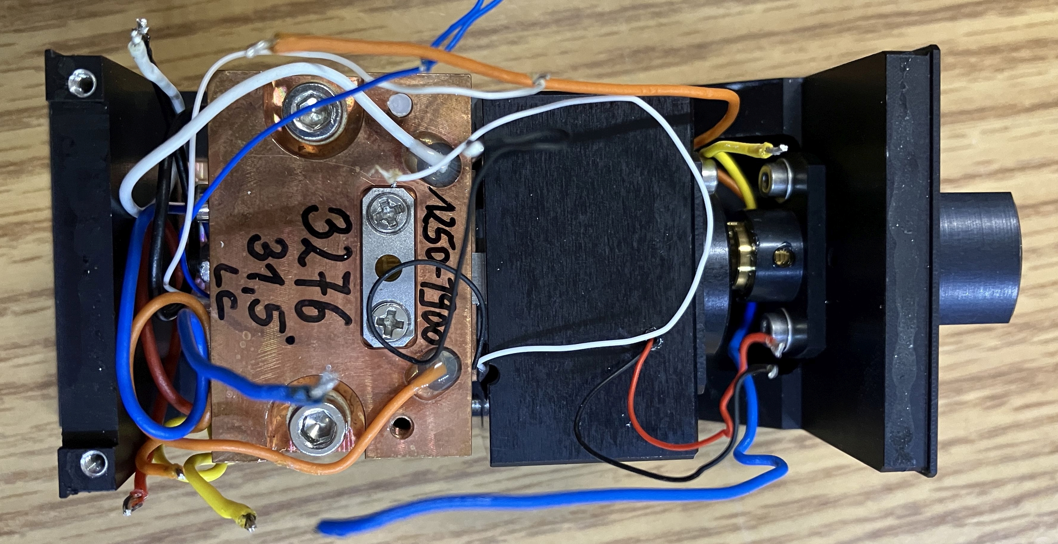
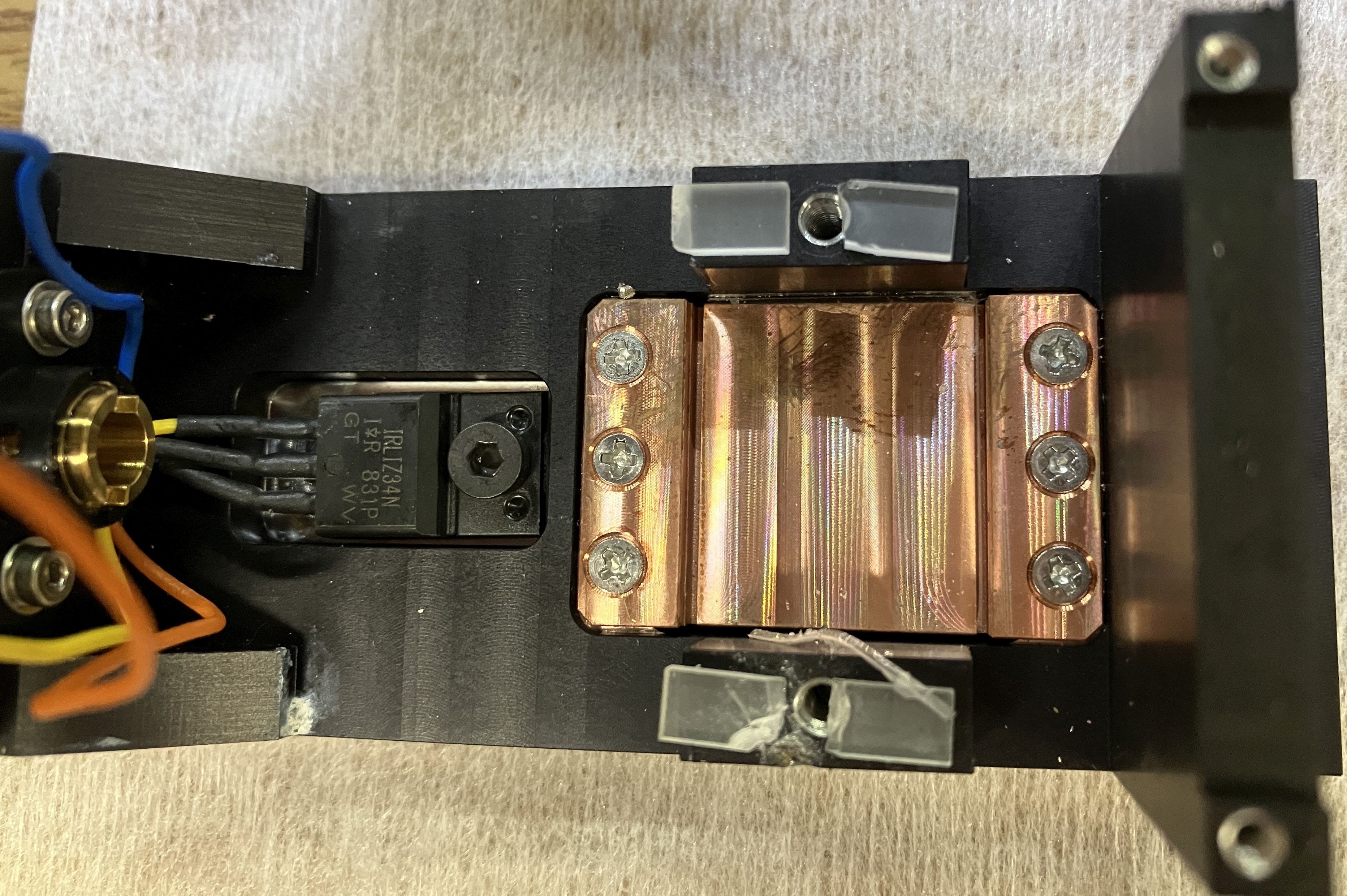
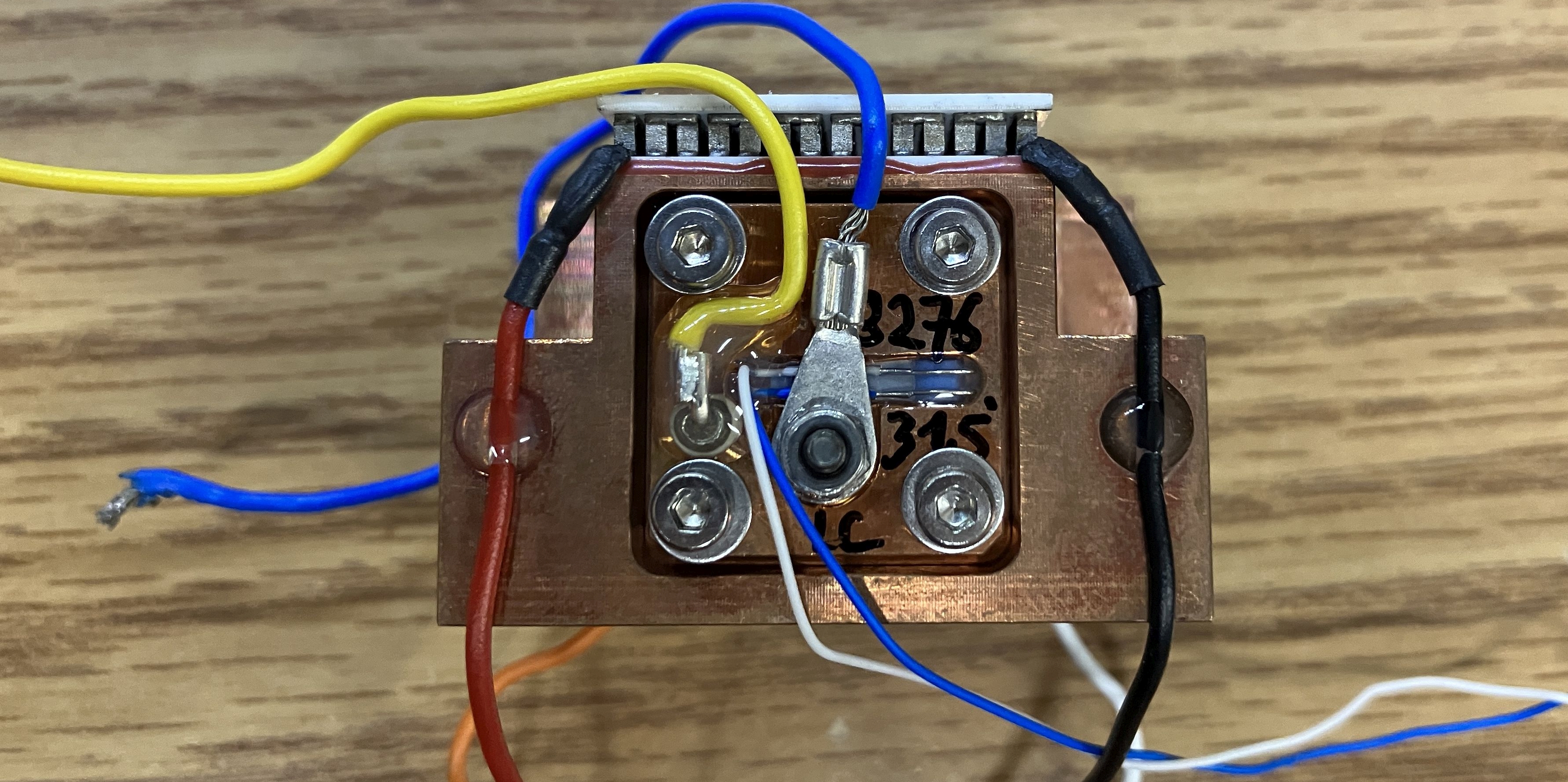
The Copper optical cavity along with the black anodized block, are mounted to the base of the laser head by two screws. There are some small glass blocks that act as spacers between the components. Be careful when torquing down the mounting screws, as these glass blocks are delicate and easy to break. They were already broken in our unit due to the radical decommissioning. The TEC sits on the copper surface of the bottom casing and interfaces with the optical cavity. The TO-220 module mounted to the bottom of the case is an Infineon IRLIZ34N power MOSFET. According to Patrick, this is used in a rather confusing manner to clamp the laser diode input for protection when the laser head is unpowered and disconnected. It is common to see a small relay inside of laser heads that use an external driver or controller. This is done to protect the diode from static discharge or other external interference, especially when the laser head is disconnected from the driver. The exposed head connector or wiring would provide an excellent path to the sensitive pump diode. The relay would be configured as normally closed, and bridge the diode anode and cathode connections together, essentially shorting the diode when the relay is not powered. Connecting a compatible controller and energizing the laser head would activate and open the relay and un-short the diode, allowing the system to operate. In the case of the LasNova 50, the N-channel MOSFET being used for this purpose is strange due to the fact that the circuit routes through a resistor on the circuit board in a rather inefficient path. This could potentially result in excess heat dissipation on the circuit board. Additionally, an enhancement-mode MOSFET was used, which activate when the gate is pulled higher than the source (similar to a normally open relay). This would essentially prevent the MOSFET from clamping the diode as intended when the system is unpowered. A depletion-mode MOSFET would (in theory) work better as a diode clamping mechanism since they are more alike a normally closed relay. Regardless, using a small relay would have been a much simpler way to achieve the pump diode protection functionality.
The optical resonator cavity contains the pump diode, lenses, and crystal stack. The c-mount pump diode is mounted on the reverse side of the square copper plate, which is secured to the resonator block by four screws. The holes on the plate are slightly oversized, which allow for precise positioning of the pump diode. The blue strip recessed into the copper plate and covered in epoxy, is a thermistor for monitoring the pump diode temperature. The TEC mounted to the resonator cavity regulates the temperature of the pump diode.
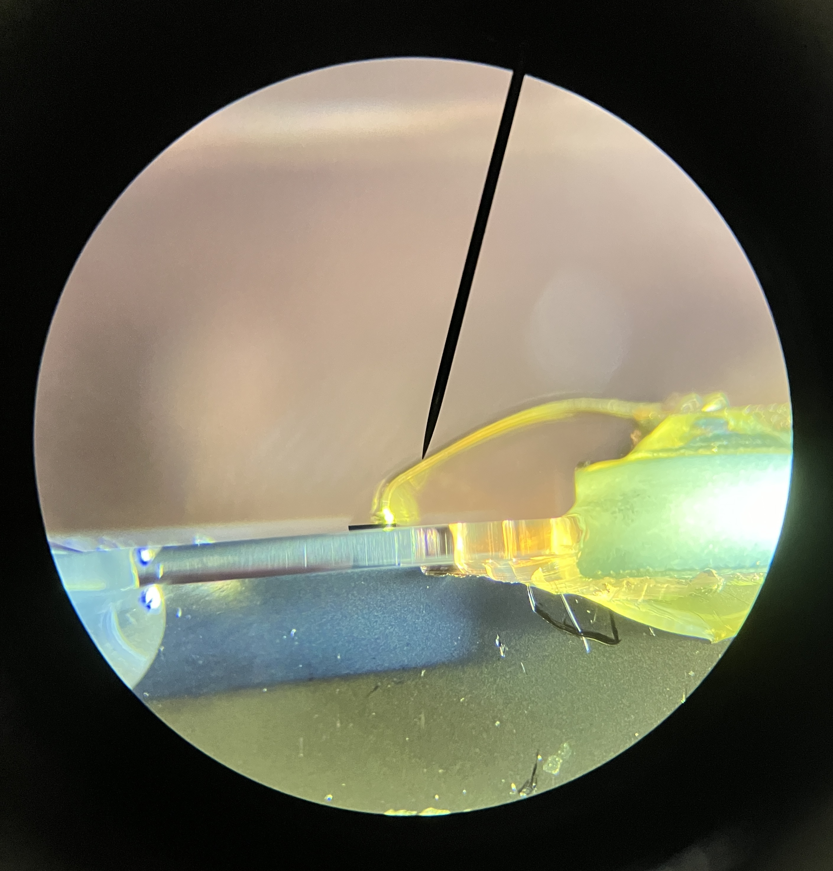
As mentioned earlier, a c-mount pump diode is used in this laser system. It is case positive, and outputs around 2W of 808nm laser light at full power. Mounted directly in front of the diode bar is a cylindrical lens called a fast axis correction lens. The FAC lens helps correct and reshape the output of the diode into a more usable, higher quality beam.
In the image below, a microscope was used to get a clearer picture of the extremely small cylindrical FAC lens. It blocks the pump diode bar which is mounted behind the lens. The gold bond-wires are visible above the lens.
This is the output side of the condensing lens, contained within the resonator block. Light emitted from the pump diode on the other side of the lens is focused down to a small point. Typically, the crystal stack would be glued to the TEC that surrounds the lens, but it was also broken off due to the damage. This second TEC (with hole in center) is responsible for regulating the temperature of the crystal stack. Also note the two screws that were sheared off due to the impact.
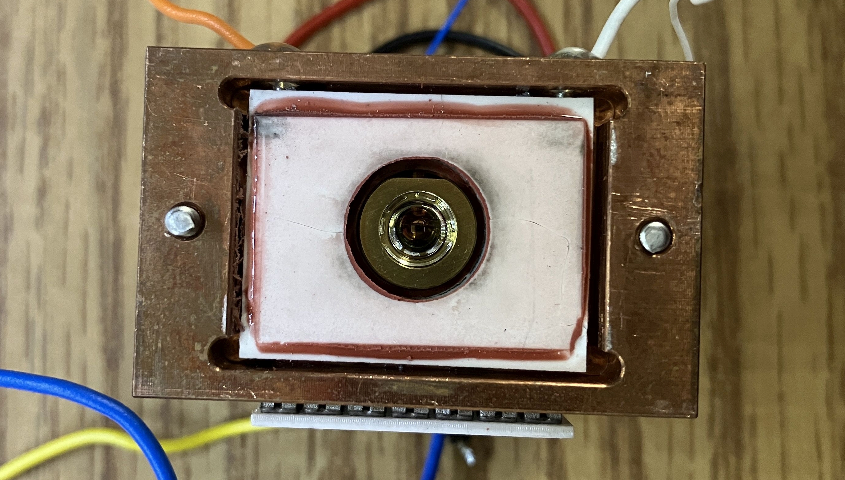
This is the input side of the crystal stack. Normally this copper surface would be bonded to the TEC pictured above. A small retention clip seems to be holding in one of the optical components in this stack.
This is the output side of the crystal stack, which is made up of two crystals. An ND:YVO4 or ND:YAG crystal converts the 808nm laser light to 1064nm. Afterwards, a KTP or LBO crystal doubles the frequency of the 1064nm laser light, which halves the wavelength, resulting in the production of 532nm laser light. This is a much more compact DPSS crystal arrangement than we are used to seeing in other laser systems. The small blue strip with the two wires is another thermistor for monitoring the crystal temperature. Nonlinear crystals are extremely sensitive to temperature and may perform poorly or not at all if the temperature is not kept within a very specific range.
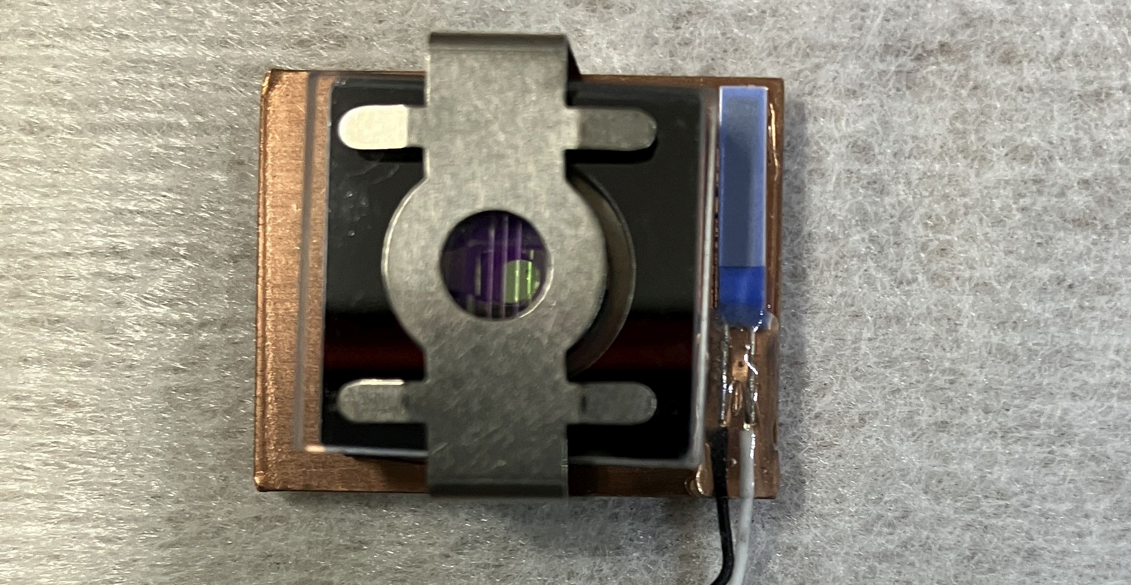
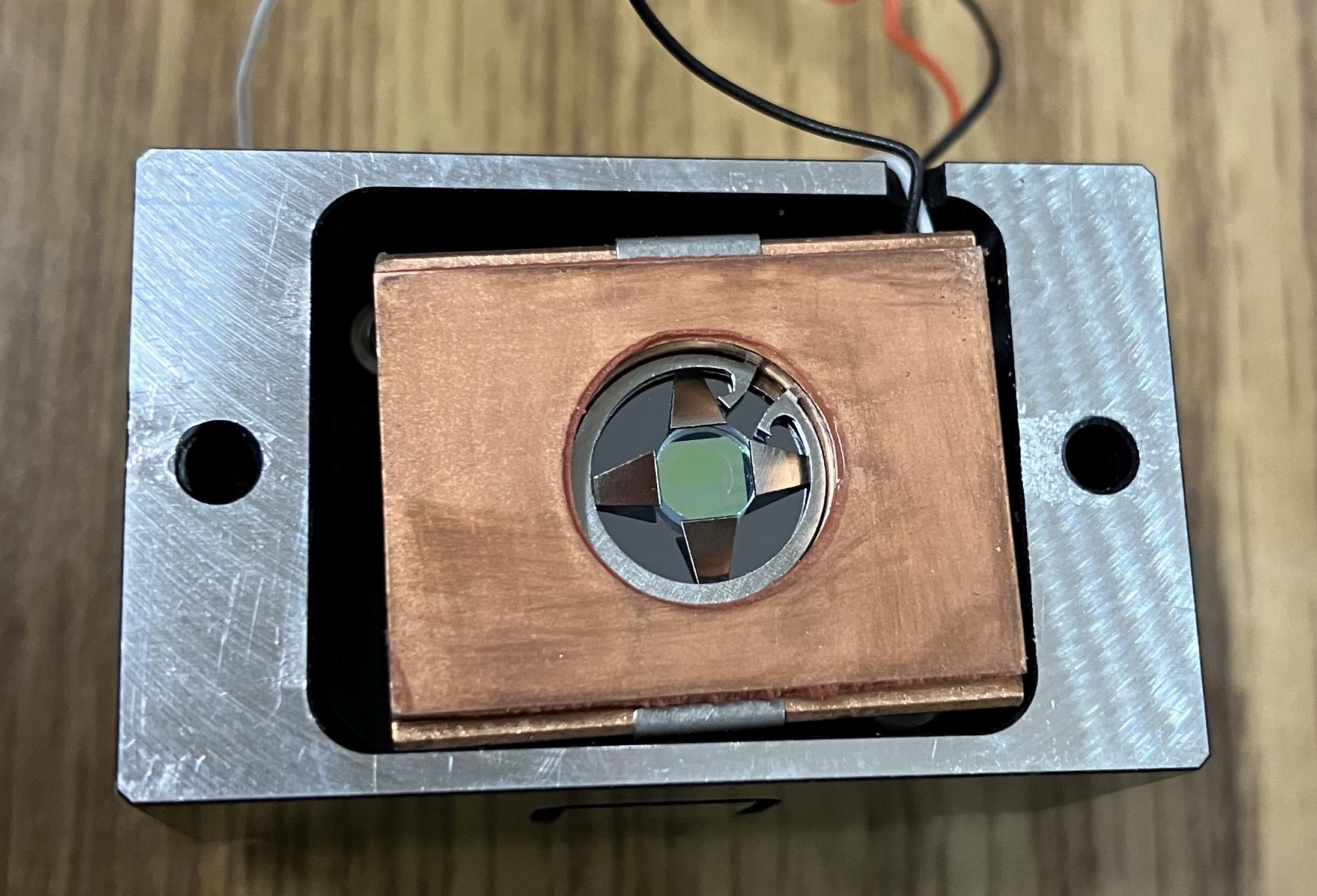
This module mounts directly to the copper resonator block and has a multiple functions. First, it contains the optical pickup or photosensor for monitoring laser output. A small filter mirror reflects a portion of the laser beam towards a photodiode that is wired to the circuit board. It seems to have a second internal filter section that is secured within the block in front of the photodiode assembly by two screws (removed in the photo below). We are not entirely sure of the purpose of this intermediate filter. Patrick thinks that it may be used to direct near-infrared light out through the black window on the side of this block for the purpose of calibrating the system during assembly.
The circular module mounted to the block contains a spatial filter, which looks like an extremely tiny pinhole aperture. The spatial filter further improves beam quality and helps to reduce divergence and speckle. Behind the spatial filter assembly is an IR filter.
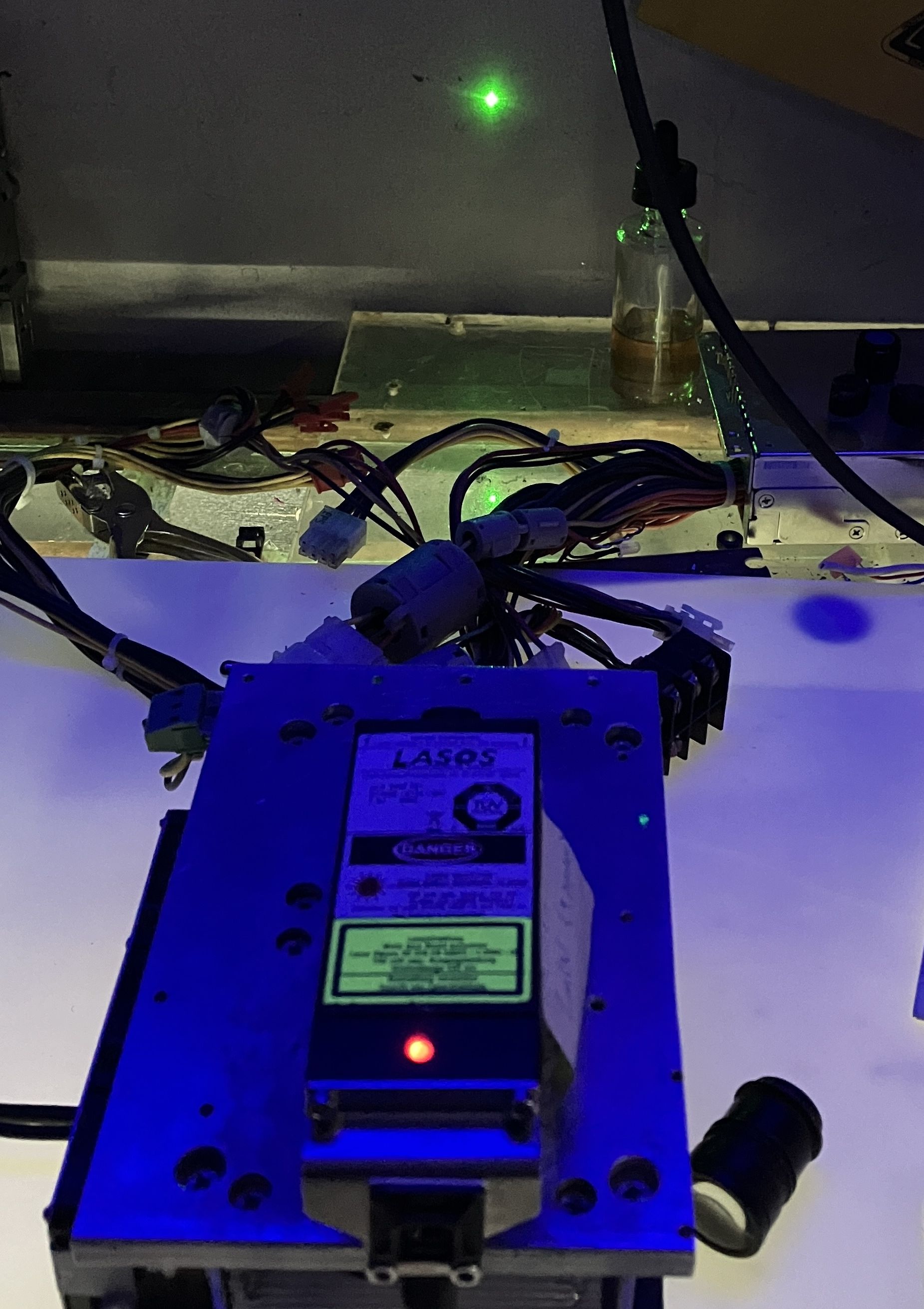
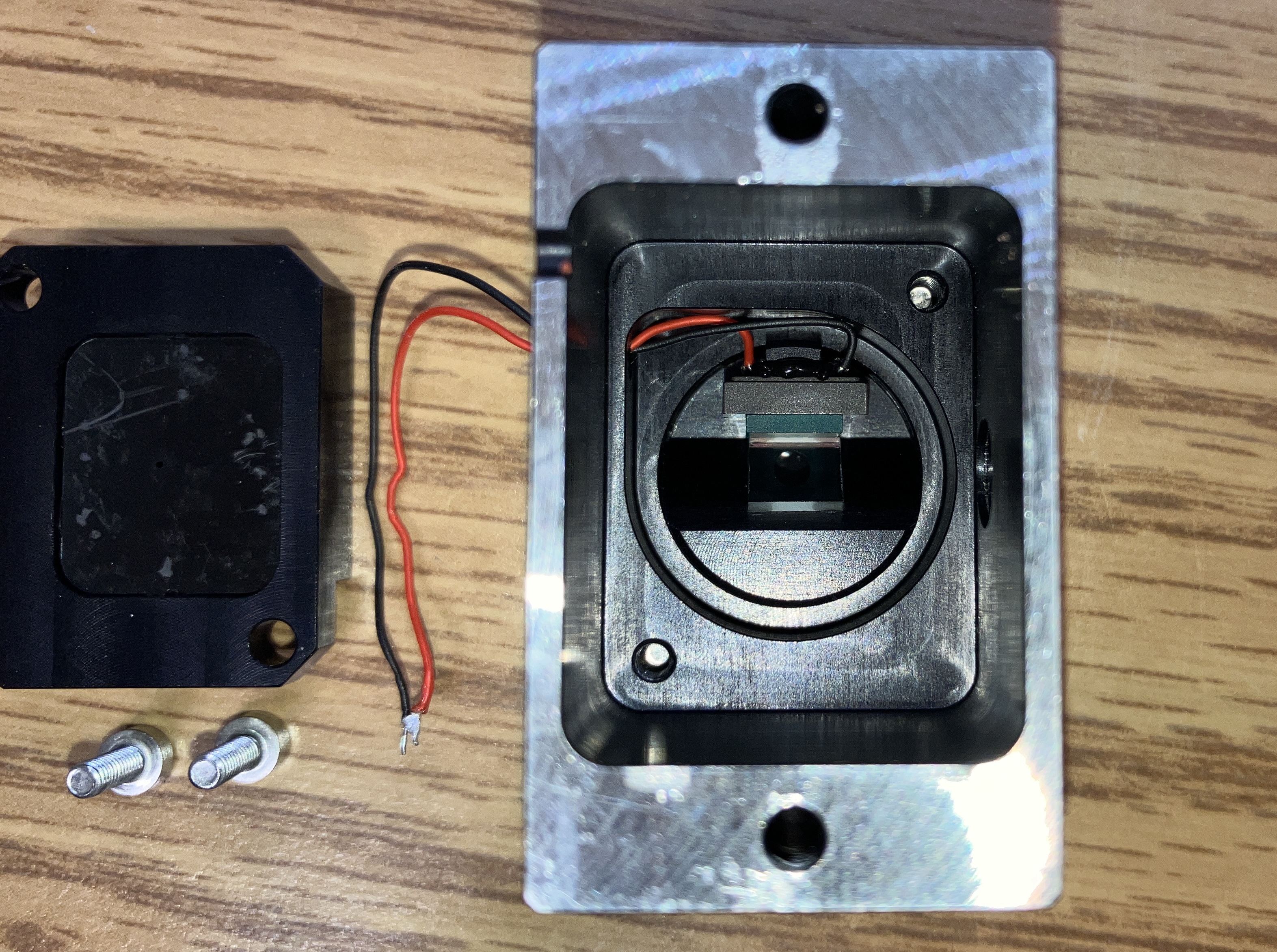
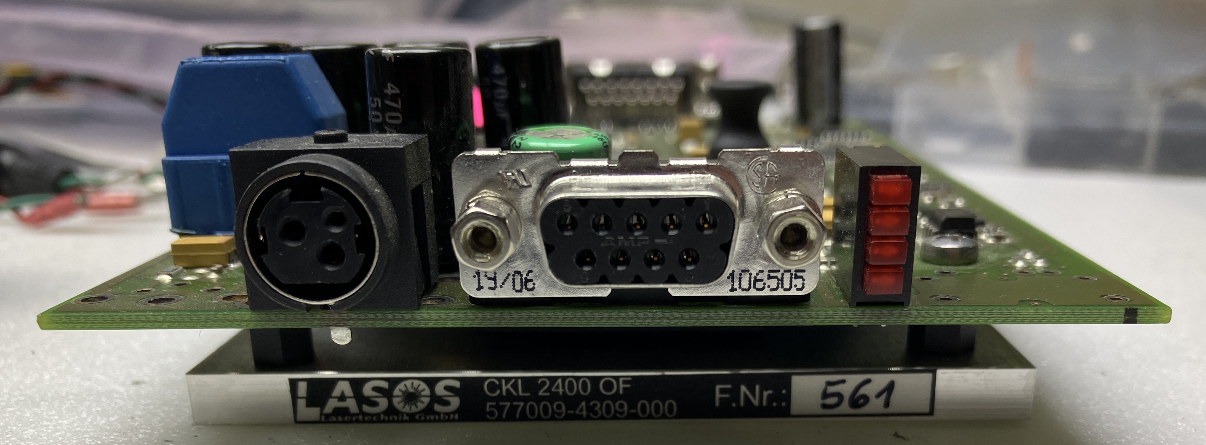
The OEM driver board used with these laser heads is a LASOS CKL 2400. The board connects to the laser head via a custom cable with a dual-row pin header socket and locking bracket for the head side, and a DA-15 connector for the driver side. The driver requires 24V DC (or 12V depending on model) input at the round, 3 pin connector. The DE-9 connector is an RS-232 serial port that allows for computer control and monitoring. LASOS has made their computer control software, Lasos Commander, freely available for download on their website along with the manual. A link to that page on their site will be provided at the bottom of this page.
Patrick was able to partially repair some of his LasNova 50 units, including one with a damaged TEC. Please check out his video which extensively covers these laser systems as well as the repair process!