This is the diode stack driver from an AMS Laserscope Greenlight HPS. It's a custom component manufactured by VueMetrix for the Laserscope, and is likely based off of their Vue-HV laser diode stack controller. This monster of a controller drives an 808nm diode stack capable of producing over 200 watts of laser light, which is used as the pump source for the 532nm DPSS laser head within the Greenlight HPS surgical laser system. The Greenlight HPS has an output power of 120-150 watts depending on the model. It's hard to say exactly how many watts the pump diode produces, but it will certainly need to be greater than the final output power due to losses experienced by any DPSS laser. We found this unit for sale by itself on eBay, the seller had removed it from a Greenlight HPS that was being parted out. This will be part of a series of writeups about the AMS Greenlight HPS (formerly the Laserscope). Strap yourself in, as this is going to be interesting!
System Overview and Teardown
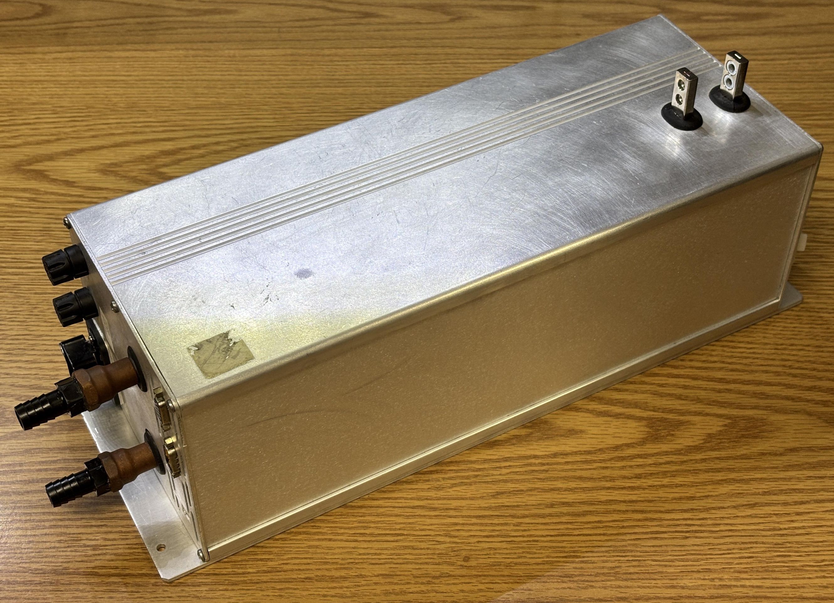
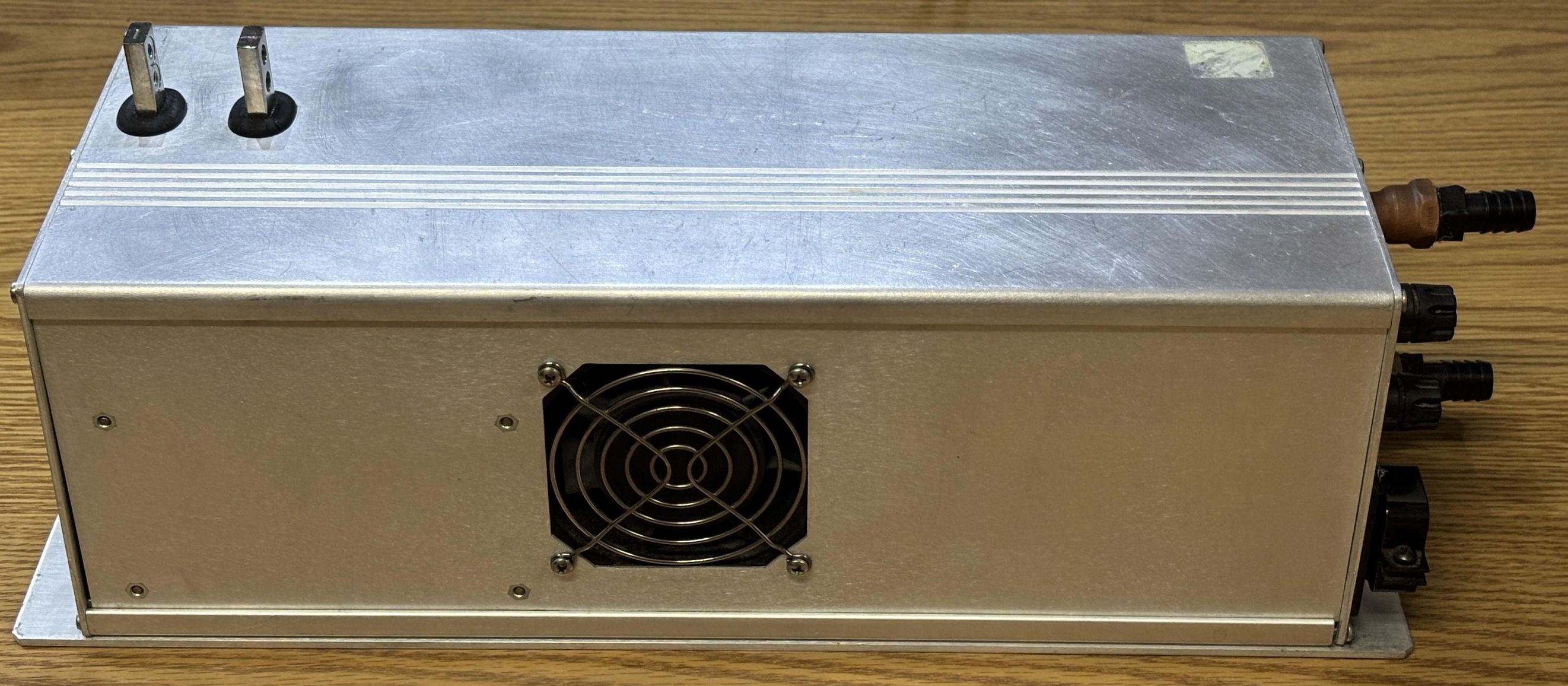
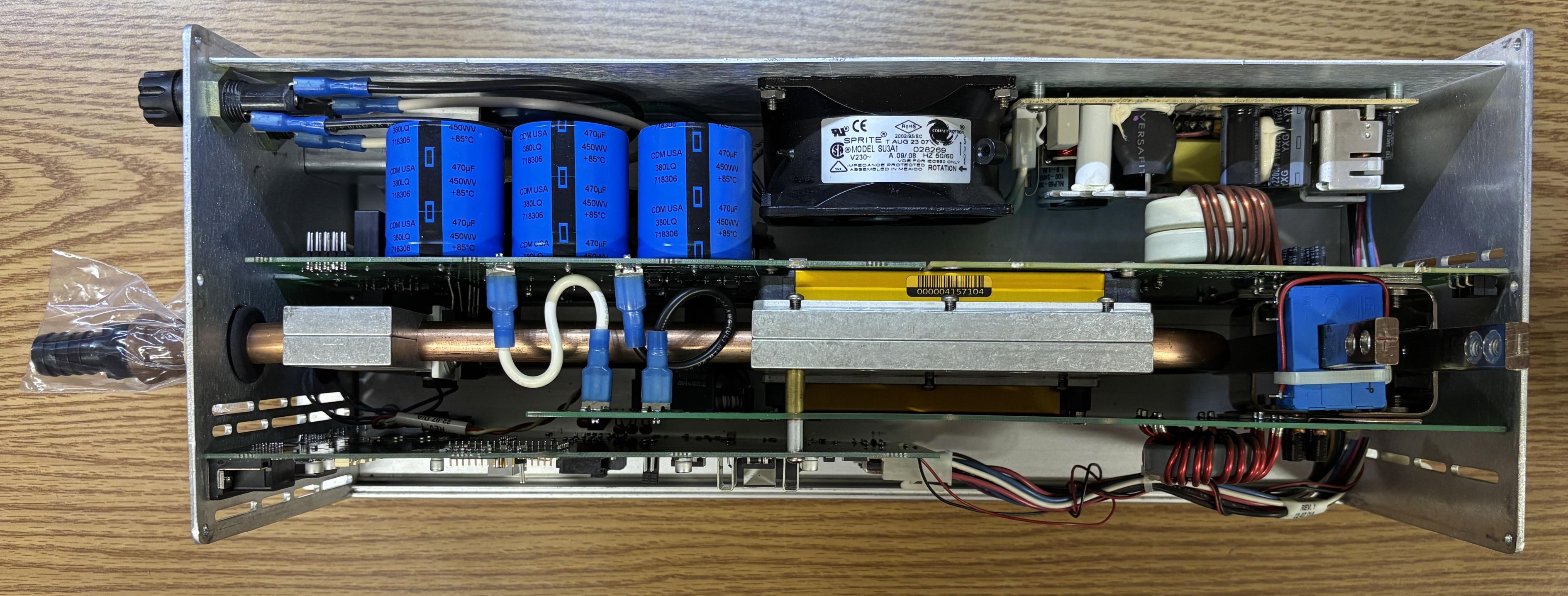
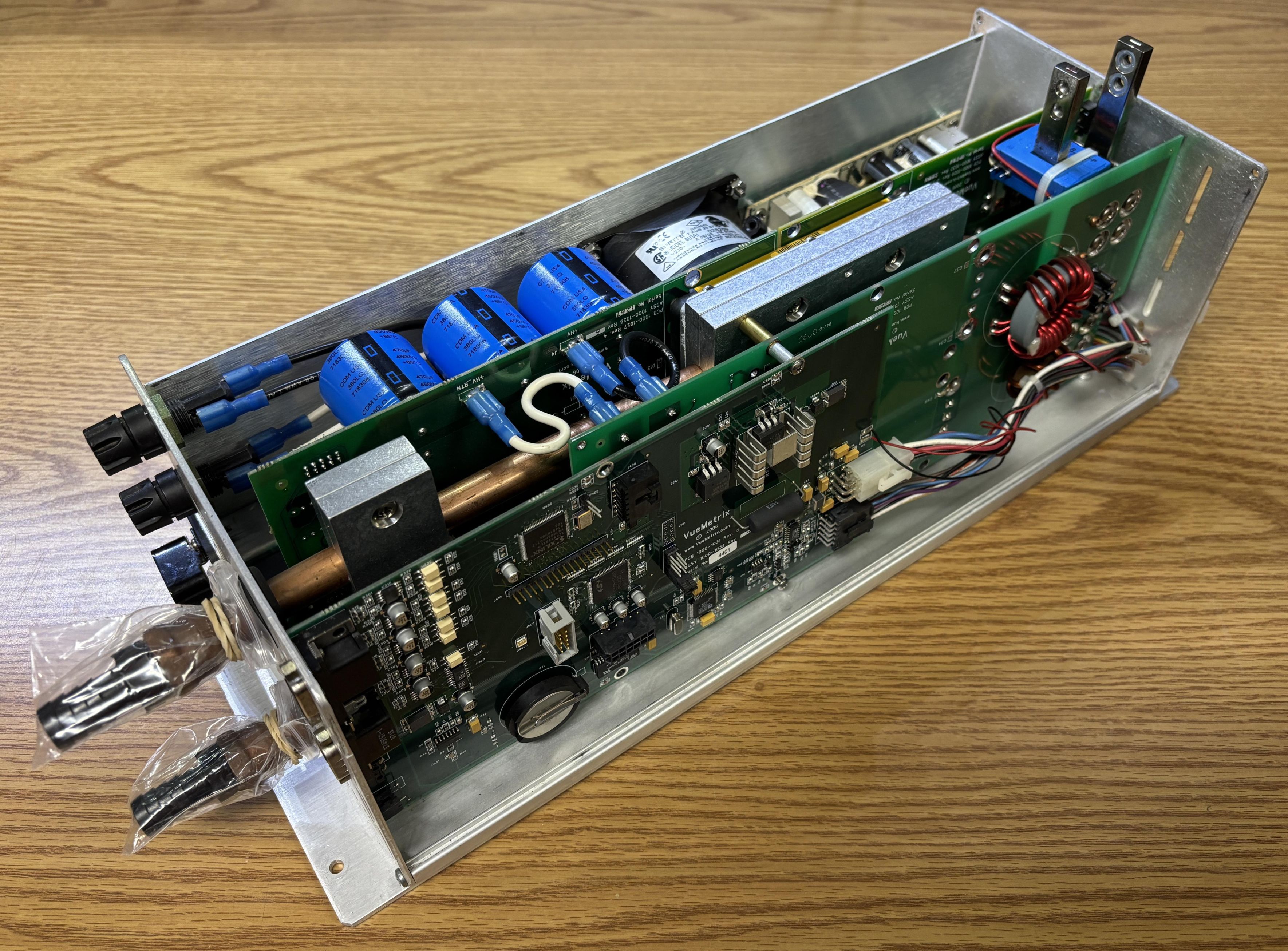
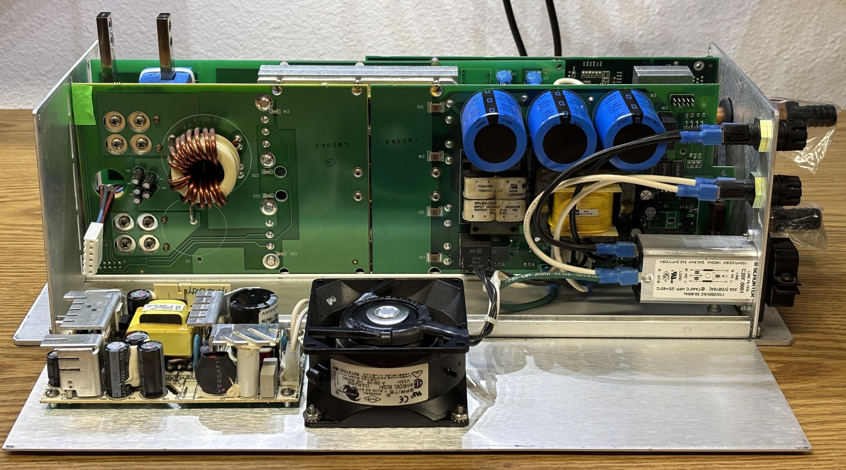
An unassuming aluminum enclosure at first, until you notice the two massive studs protruding through the top. Those are for the laser diode stack. They are designed to carry many of amps of DC current, at a maximum voltage of around 15 volts. The fan is misleading as that's just to cool the electronics within. The DC-DC converters that actually drive the diode stack are water-cooled as evident by the two copper pipes sticking out of the side.
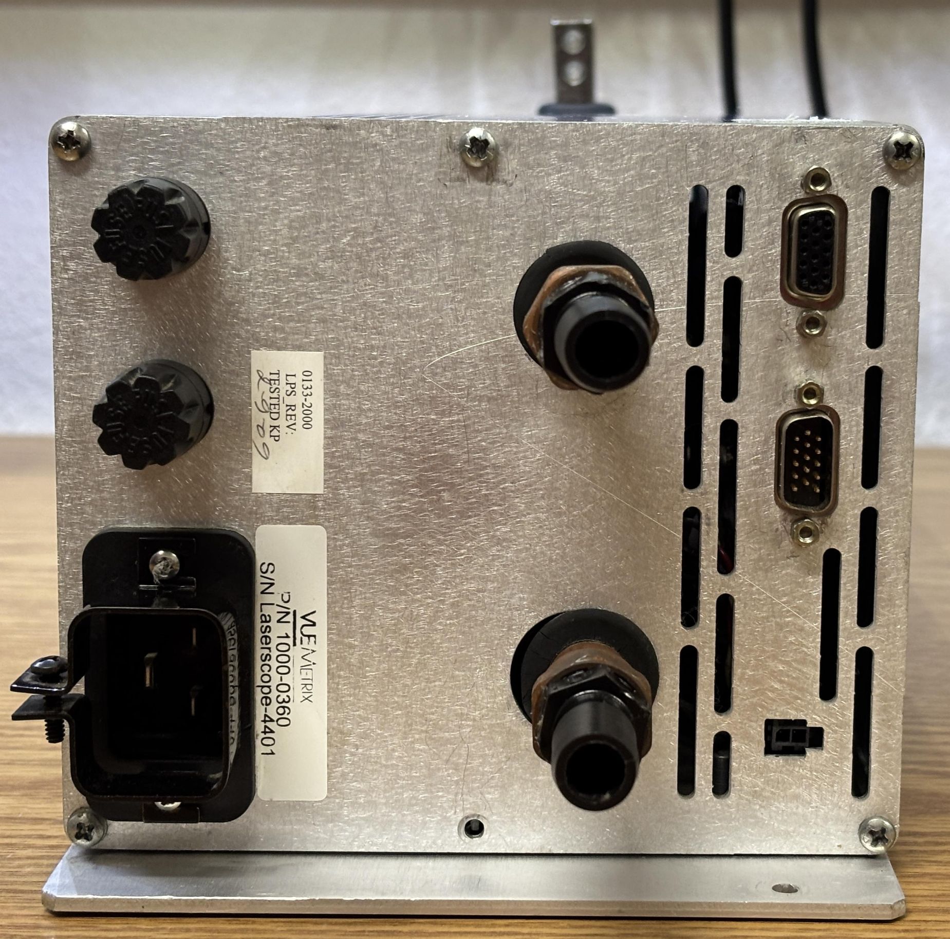
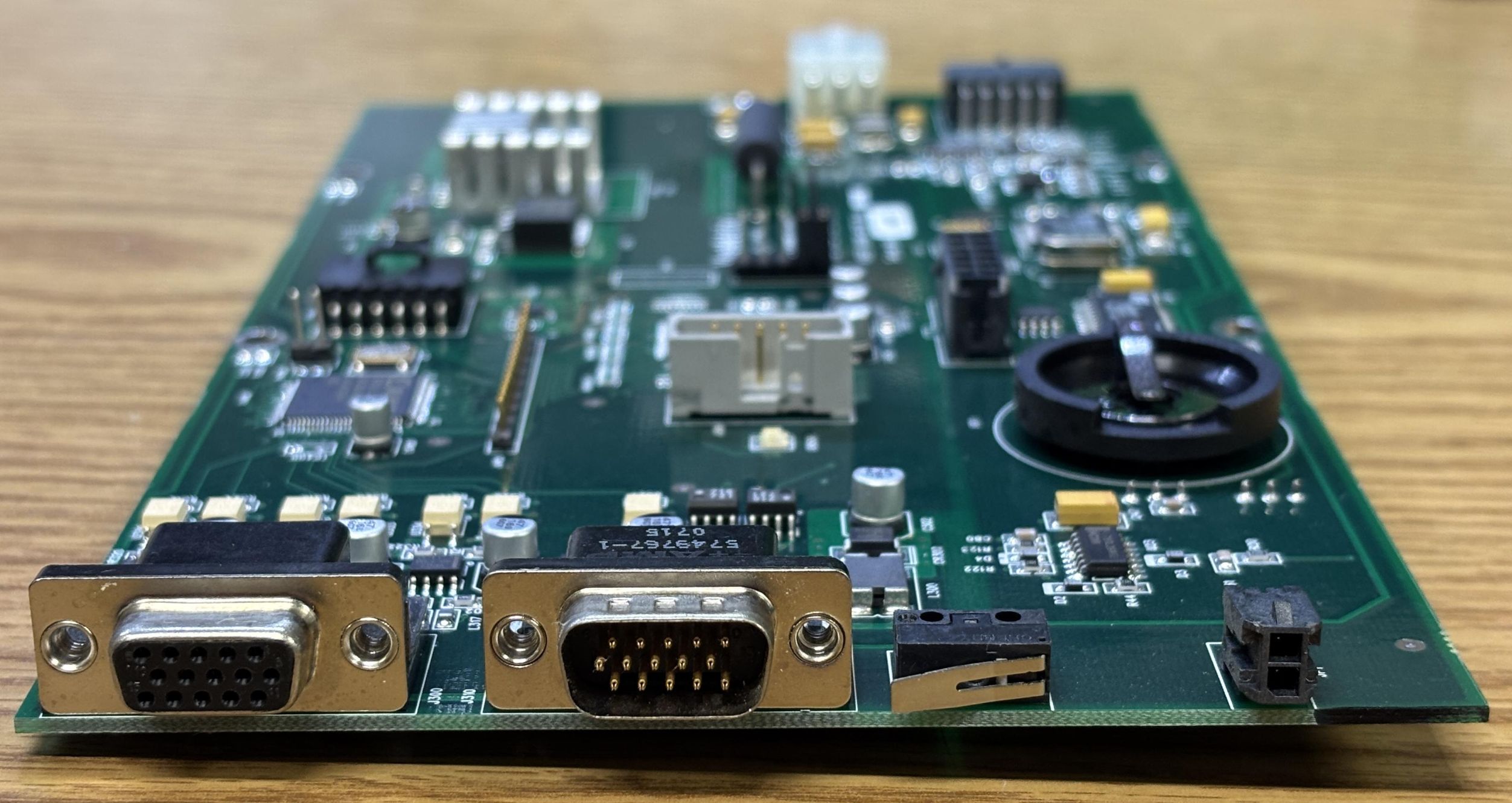
For the AC input, it uses a 30-amp IEC connector and is designed for 240V AC operation, single-phase. It has two removable fuses to protect the input side. Most notably are the two copper pipes with plastic hose barbs installed, which are for the water inlet and outlet. This diode driver, along with the diode stack and q-switch, is water-cooled by a closed-loop chiller and pump installed in the Greenlight HPS. According to the published specifications for the Vue-HV controller, 1 GPM @ 10 PSI, 15-35 °C was required to keep the unit adequately cooled during operation. For digital control, there are two DB-15 connectors, one male and one female. These carry both CANBUS and RS-485 data and is where the Greenlight HPS gets irritating. The diode driver uses both communication protocols in a complex arrangement for monitoring and control by the rest of the system. The small 2-pin Molex connector below the DB-15 connectors is just a discrete interlock connection. According to the label, the part number for this device is 1000-0360.
Removing the top row of Philips screws on either side of the unit allow the top cover to be pulled away, which then releases both side panels. They are just thin pieces of aluminum that are secured in channels on the top and bottom sections of the casing. Here we get our first look at the internal components of this diode driver.
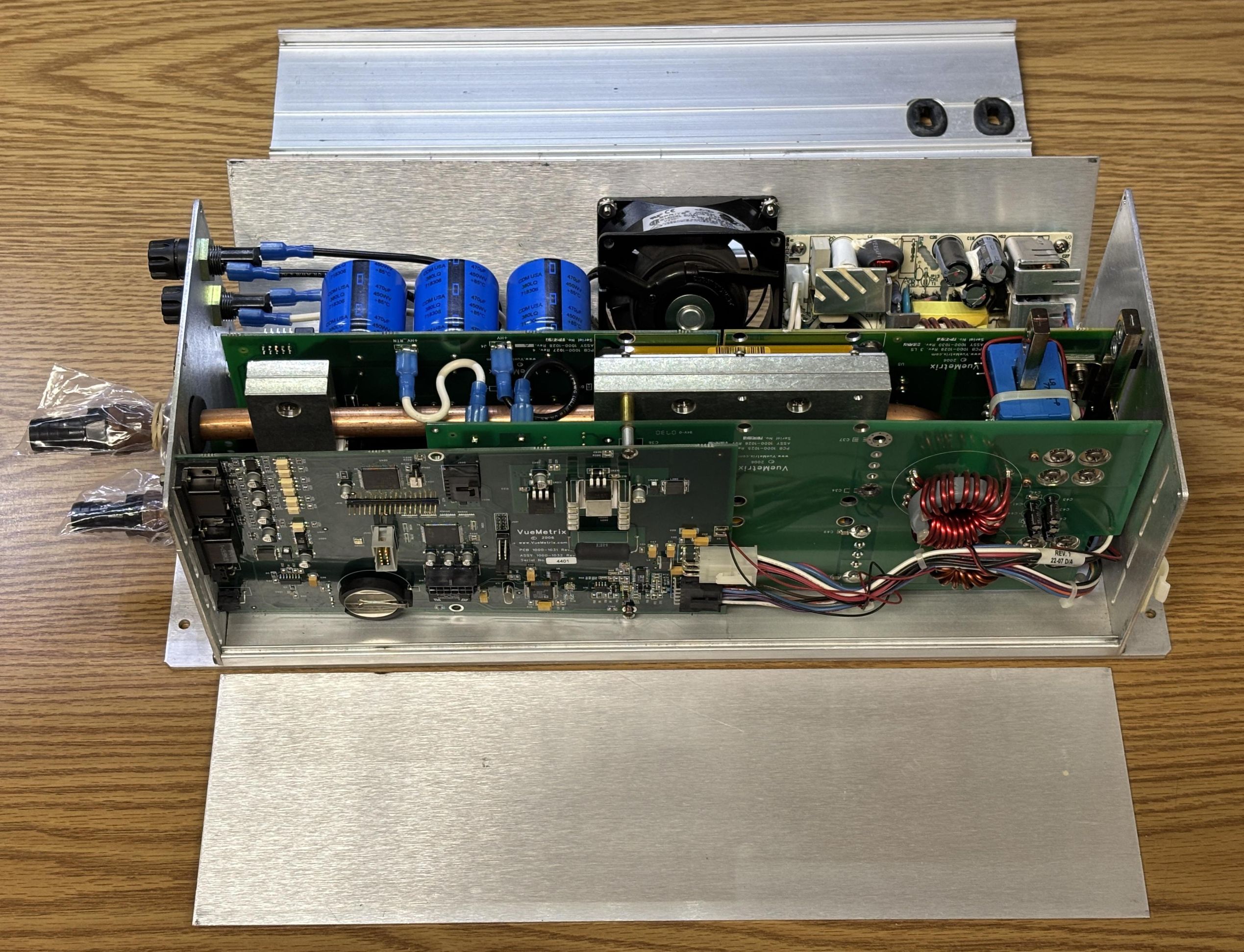
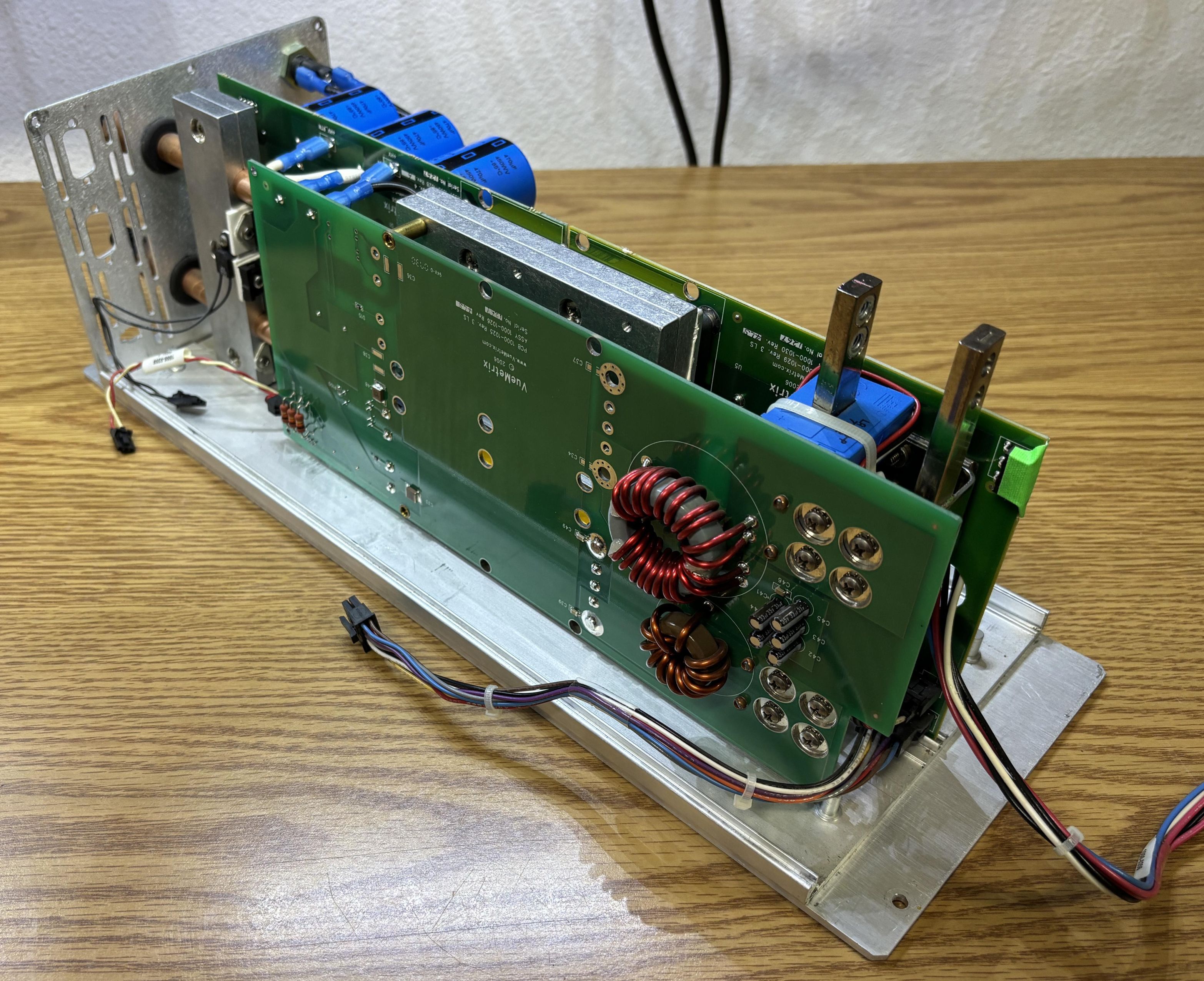
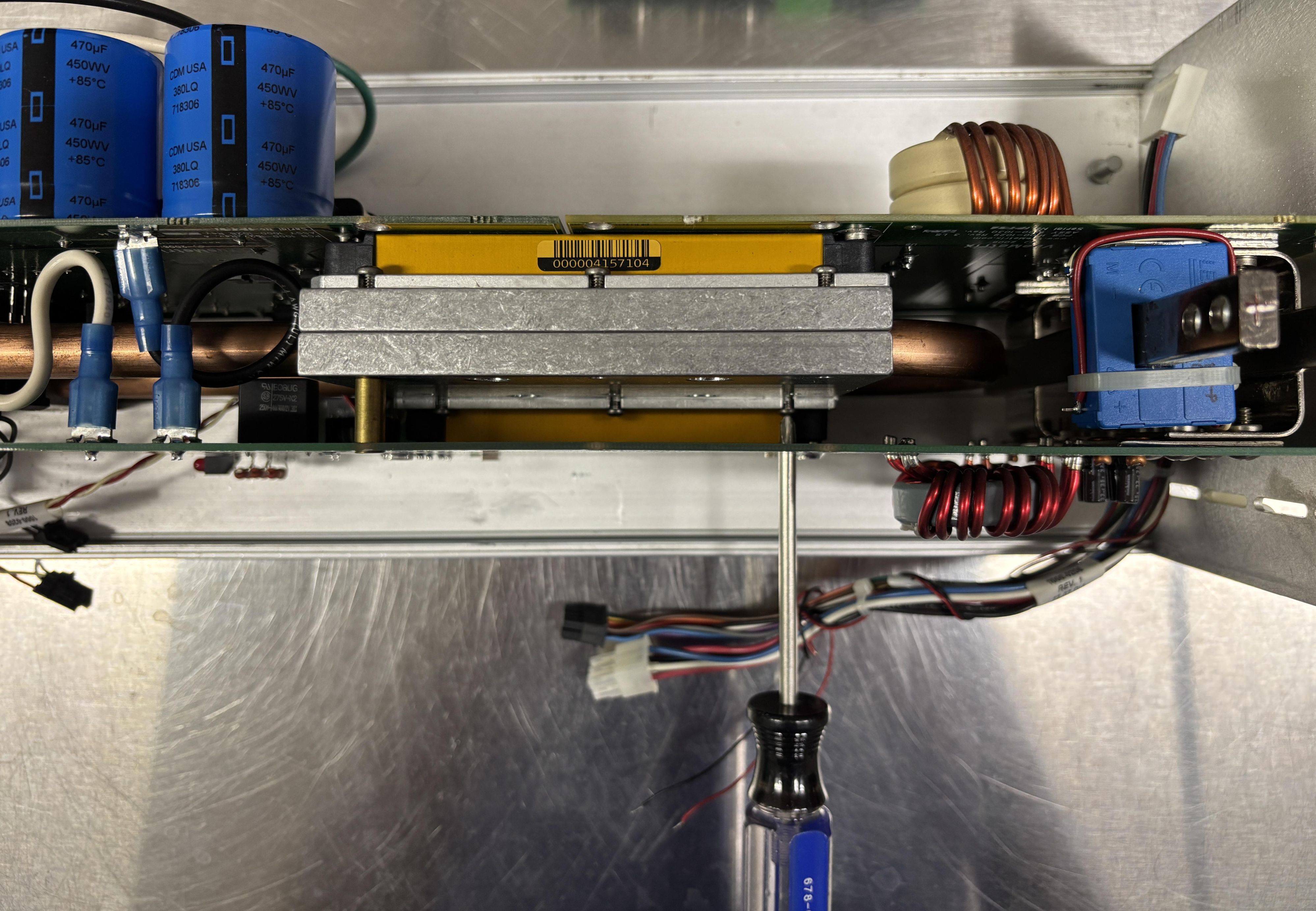
The driver contains a stack of boards that include three water-cooled DC-DC converter modules mounted to separate PCBs. Also, there is a low-voltage power supply, fan, PFC circuit, and a digital control board.
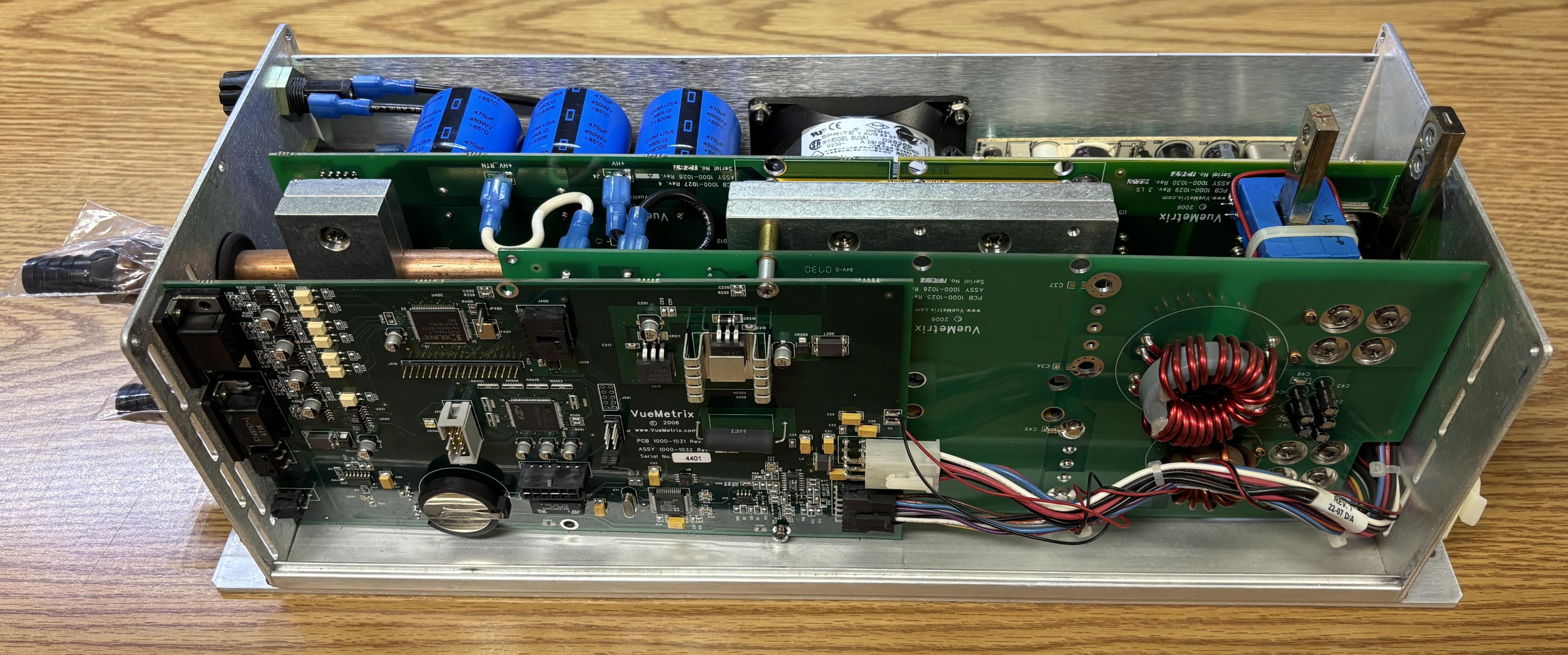
Components top to bottom: fan & low-voltage power supply, rectifier & primary DC-DC board, heatsink and water cooling lines, secondary DC-DC board, digital control board.
It's pretty tightly packed, and impressive that they can get away with a driver this small that can deliver 120 amps of current to the diode stack. That is certainly due to the usage of liquid cooling. An air-cooled driver of similar capability would be significantly larger due to the heatsinks required for adequate heat dissipation.
Here is a closer look at the two diode connection studs, inscribed with polarity markings. Each stud has two threaded inserts used to attach the braided leads for the diode stack. The blue module is a LEM LA 100-P hall effect current transducer, which is used to report the output current directly to the digital control board.
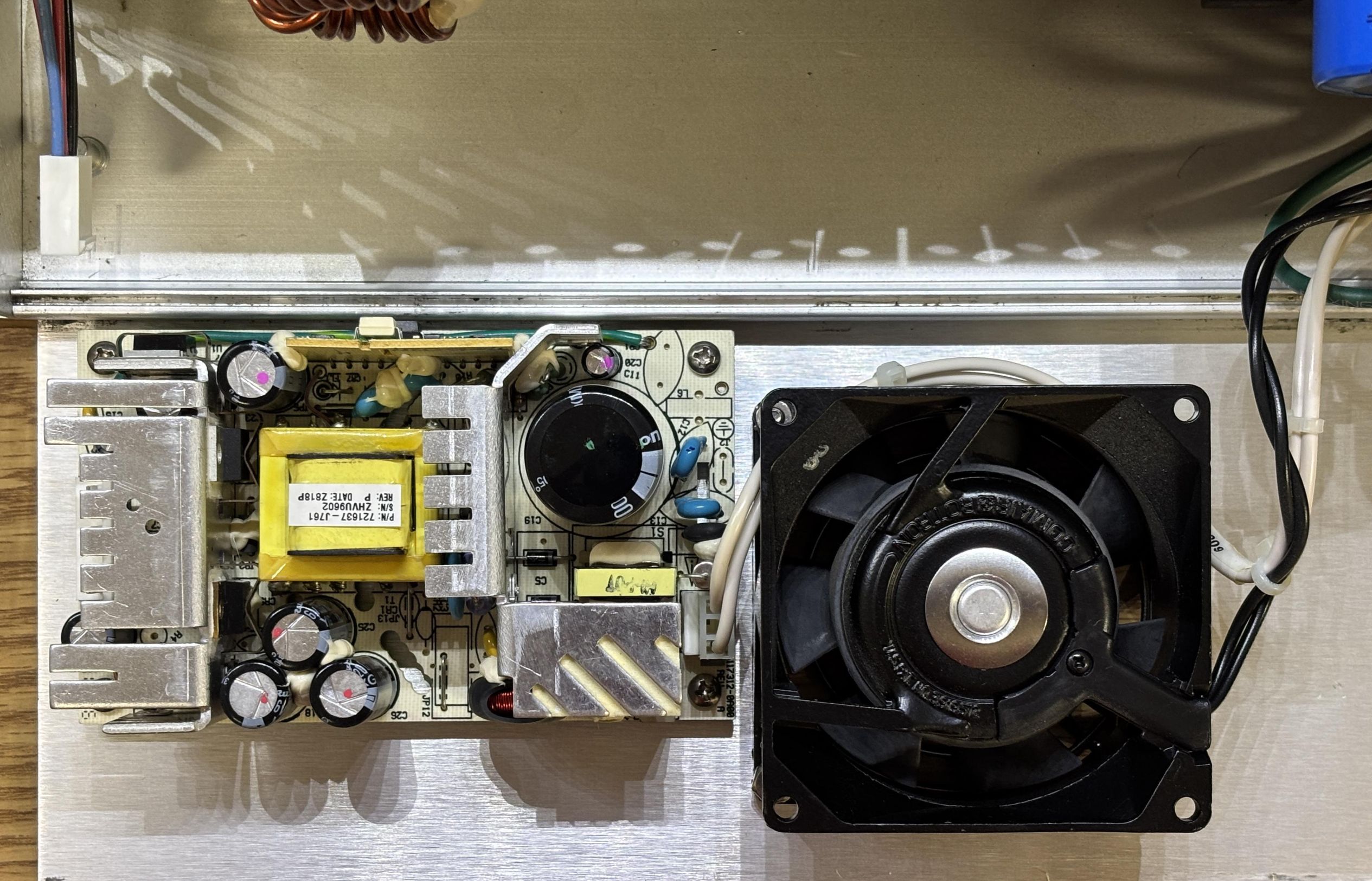
The fan and low-voltage power supply are attached to the aluminum panel on this side. There is enough cable length to allow it to hinge away from the rest of the assembly. The fan is just used to cool the electronics, not the DC-DC converters regulating power to the diode stack.
The low-voltage power supply is an Artesyn NLP65-7608J (triple-output) which is used to provide power to the digital control board exclusively. It has three DC output rails: 5V, 15V, and -12V. The fan is a Comair Rotron SU3A1 and is powered directly by the 240V AC input.
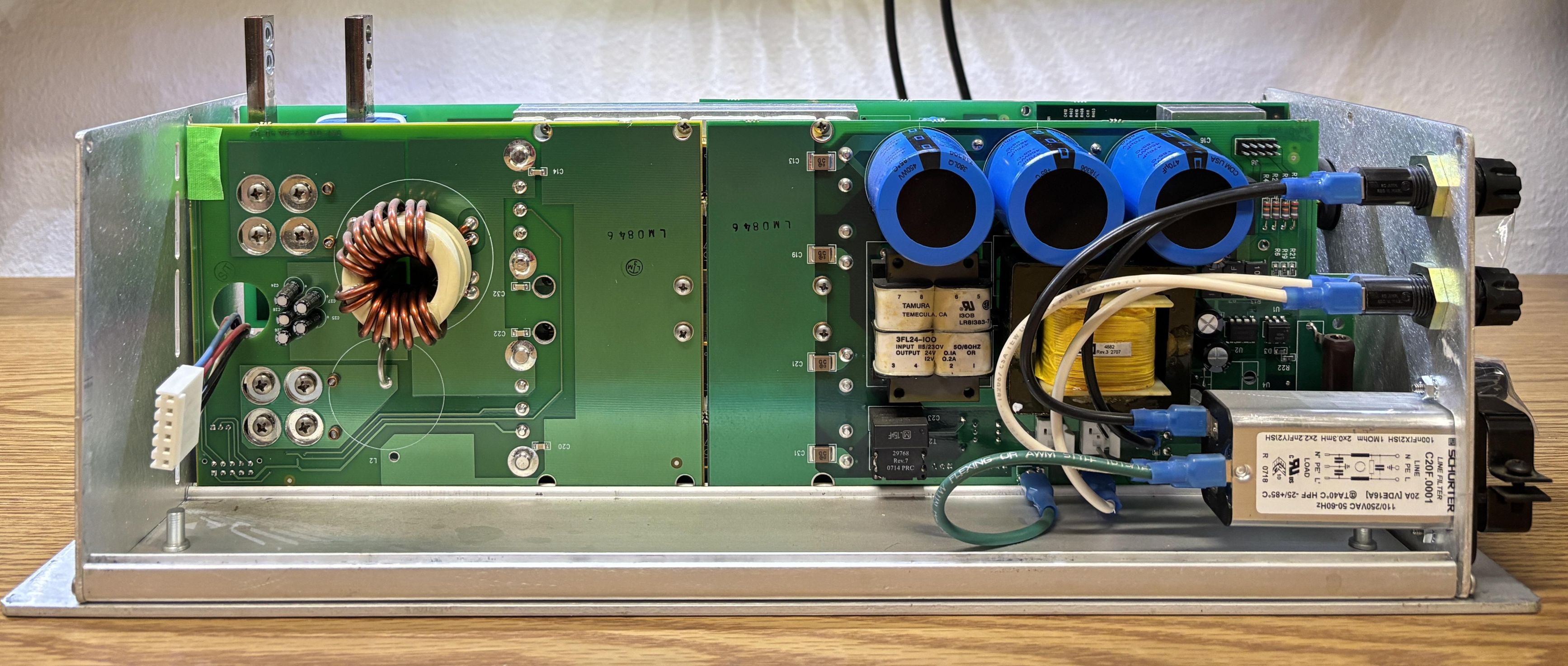
This PCB is part of the AC input section which includes two fuses, an AC line filter, three large capacitors for smoothing, a PFC circuit, and a rectifier for converting the AC to DC. On the other side are two DC-DC converters. Take note of the isolation slot in the center of the board, essentially breaking it into two separate boards.
The digital control board is attached to the rest of the assembly via two threaded standoffs and screws along with the retention nuts on either side of both DB-15 connectors.
With most of the metal panels and the digital board removed, we are left with the core of the diode driver.
Digital Control Board Analysis
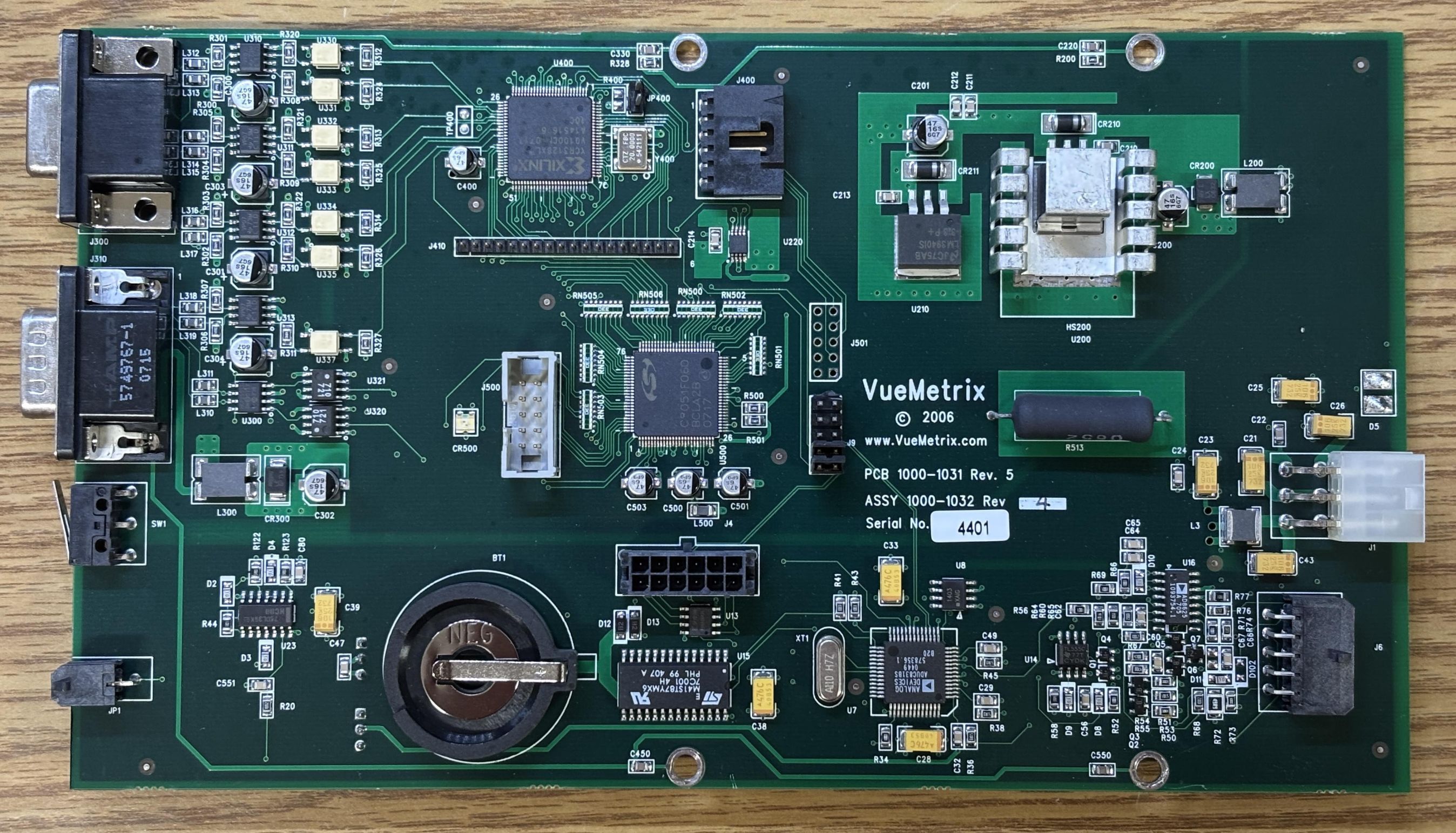
This is the digital control board. Based on documentation from the VueMetrix website, now available through the Internet Archive, the Vue-HV diode driver would have been controllable over USB or RS-232 with commands or their GUI software. VueMetrix actually did a great job of publishing their software, documentation, and commands reference right on their website. However, we don't have that luxury with the AMS Laserscope version of this driver as the original digital control board was replaced by a custom board specifically developed for AMS. The AMS board communicates over CANBUS and RS-485, not USB or serial, and has a part number of 1000-1031. There is constant communication over the CANBUS network, which is how it reports its status to the other components such as the main control board and data logging board. It also monitors the CANBUS for shutdown and emergency signals which can be used to halt emission or cut off power to the diodes completely. It is our understanding that current set points and most direct control is achieved through the RS-485 connections.
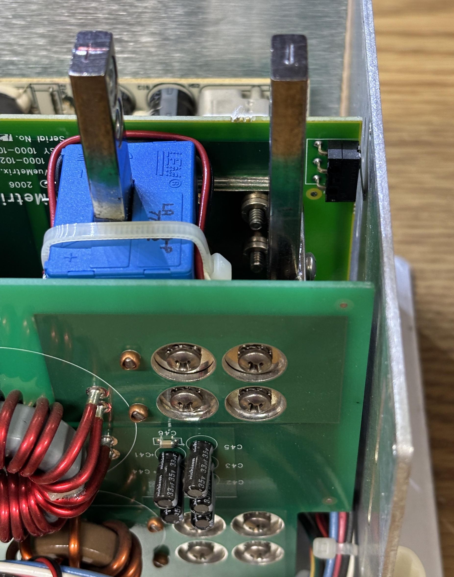
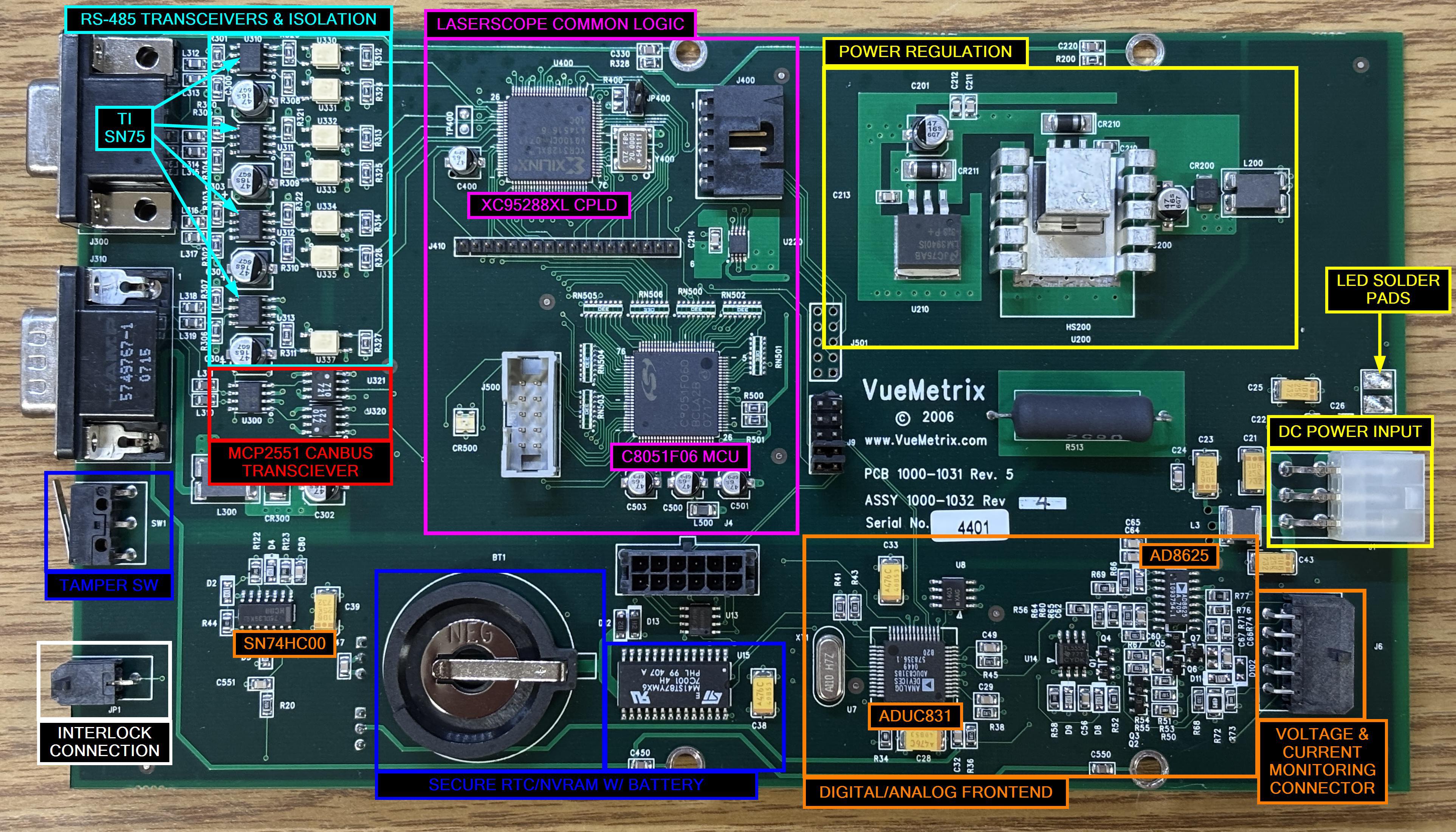
This board is quite complicated, so we broke it up into sections. There is a DC power regulation section (yellow outline) that is fed by the white 6-pin Molex connector. There is a 10-pin Molex connector which is for the voltage and current monitoring inputs from the DC-DC converter boards. Right above the white Molex connector are a couple solder pads for a status indicator LED. The section outlined in magenta is what we call the Laserscope common logic. This consists of a XILINX XC95288XL CPLD and a Silicon Labs C8051F060 MCU along with some supporting components and pin headers for programming. This arrangement of components is present on several other modules within the AMS Greenlight HPS, and is likely where they implement their custom software controls. It's basically all a mystery since there is no external EEPROM and the chips are surely to be protected from firmware read operations. The section outlined in cyan contains four SN65HVD0 RS-485 transceivers, likely implemented in a full-duplex arrangement for control. The section outlined in red contains a MCP2551 CANBUS transceiver. The usage of both RS-485 and CANBUS is interesting, likely for redundancy but also different functions. Both are very reliable industrial communication protocols. The blue section is the most sinister, it includes a tamper switch, a CR2330 battery tray, and a ST Microelectronics M41ST87Y secure serial RTC and NVRAM supervisor with tamper detection. This chip also has 128 bytes of clearable NVRAM and an integrated crystal oscillator. A component like this makes no sense in a laser diode driver. The only place we have seen similar chips is within credit card payment terminals, for storing the encryption keys. Most likely, AMS wanted to prevent aftermarket usage or "hacking" of the diode driver. It is unclear what level of security they have implemented. Based on our analysis, the CANBUS data is not encrypted during transmission, but we also do know that the diode driver will not communicate if the coin-cell battery is dead. We also don't fully understand what effect the tamper switches have. They may erase a portion of the NVRAM and brick the device, or they may just log a tamper event. Regardless, bypassing that nonsense is the most efficient way to get one of these diode drivers up and running. Read on, as it's actually quite simple.
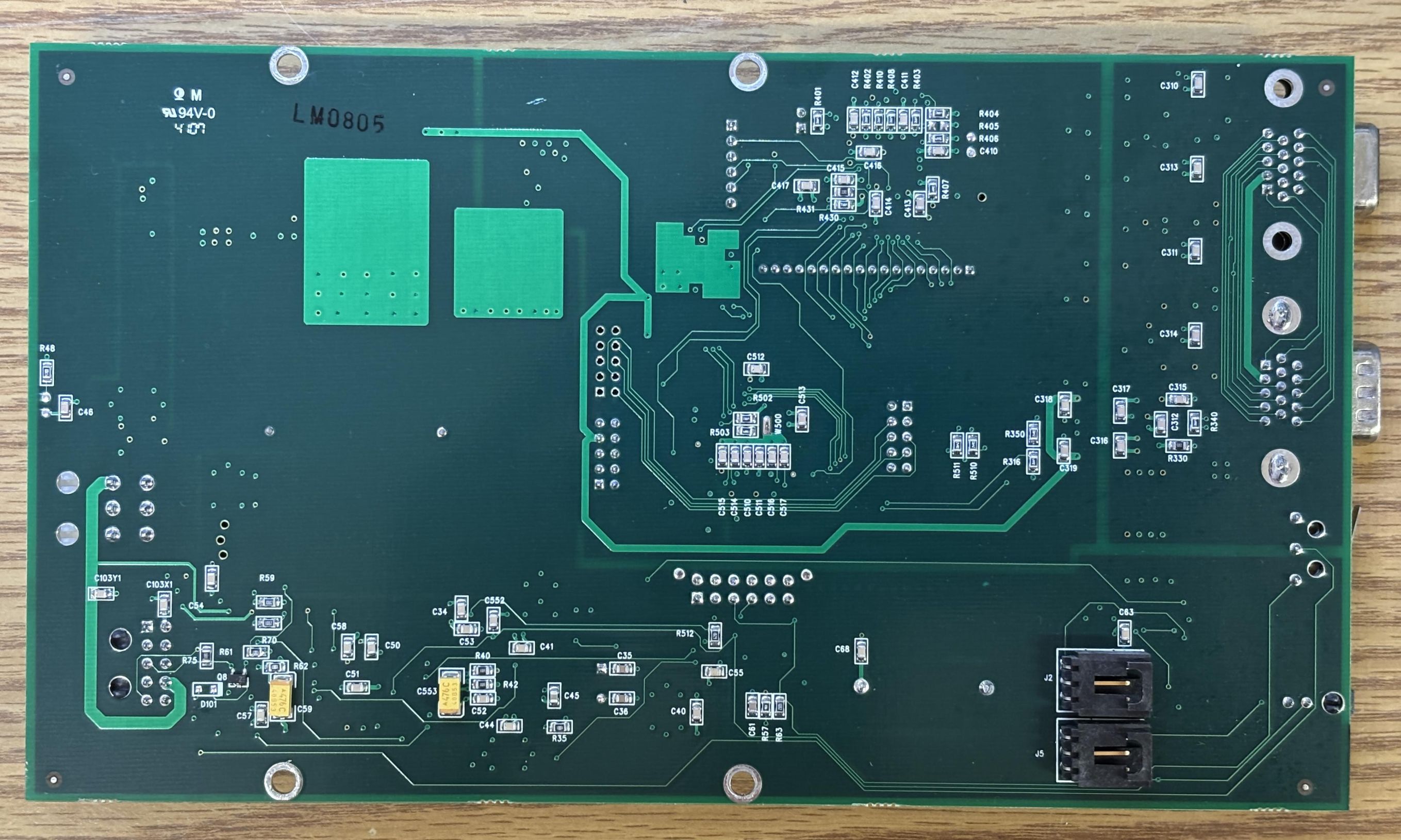
On the back of the digital control board, there are not many notable components other then the J2 (diode power control) and J5 (heatsink thermistor) connectors.
As mentioned earlier, the diode driver board has two DB-15 connectors. One goes directly to the main control board, and the other is a dedicated connection for the data logging board (DLB). While logging CANBUS data, we observed the diode driver outputting a calibration table of power set points and current values, which is likely being recorded by the data logging board. This could be used to ensure compliance if the system were to be analyzed after an incident. The small 2-pin Molex connector is for an interlock connection. Lastly, the micro-switch is one of two tamper switches installed in this diode driver. When the digital control board is installed in the aluminum casing, this switch is depressed against the side panel, and is not accessible or visible from the outside. We believe this to be a tamper switch due to the presence of the secure storage module and the fact that the switches won't be released if the top cover is removed, only the sides. It if was a safety interlock, we'd expect it to detect the removal of the top cover as well, not just the sides.
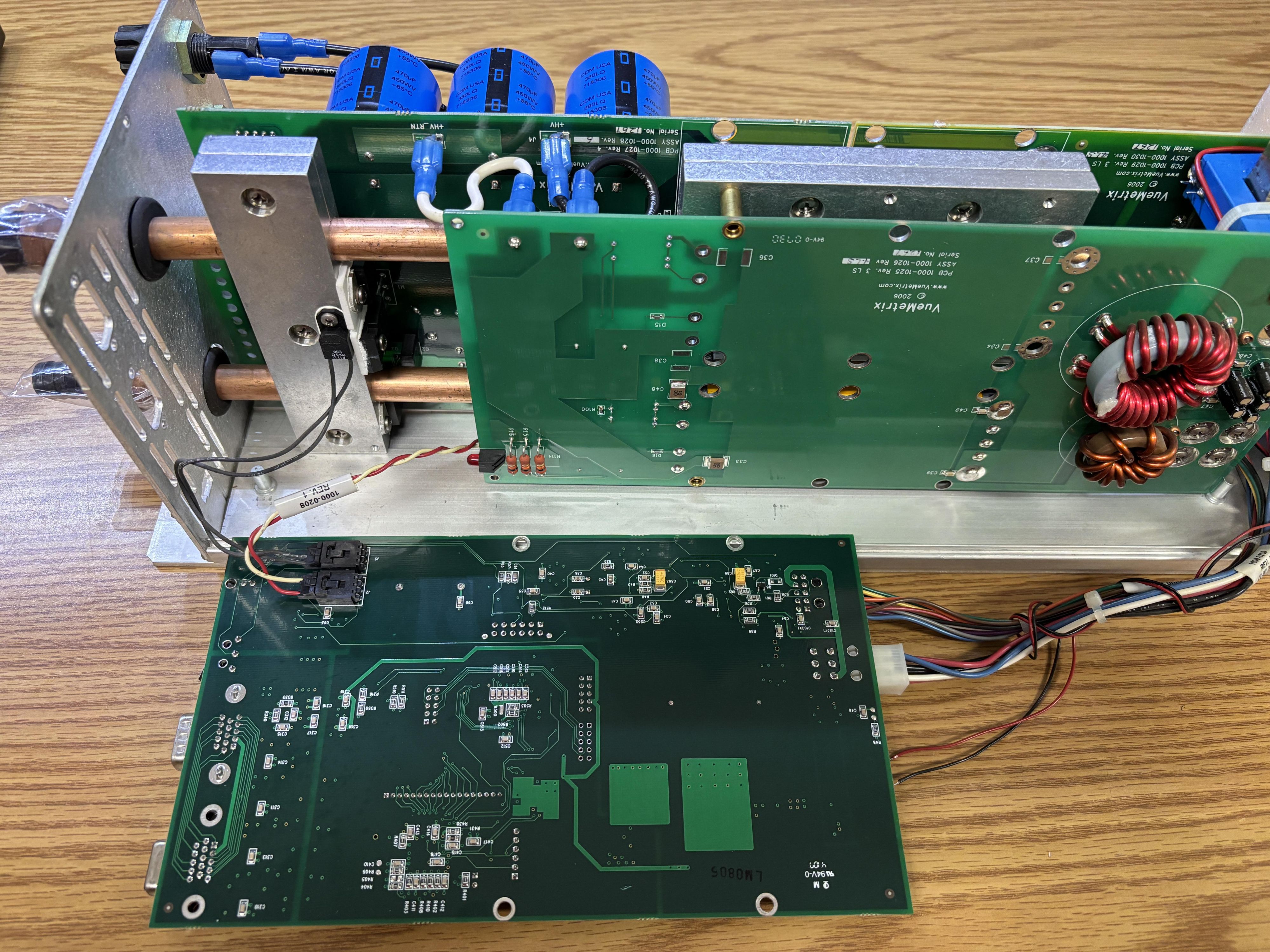
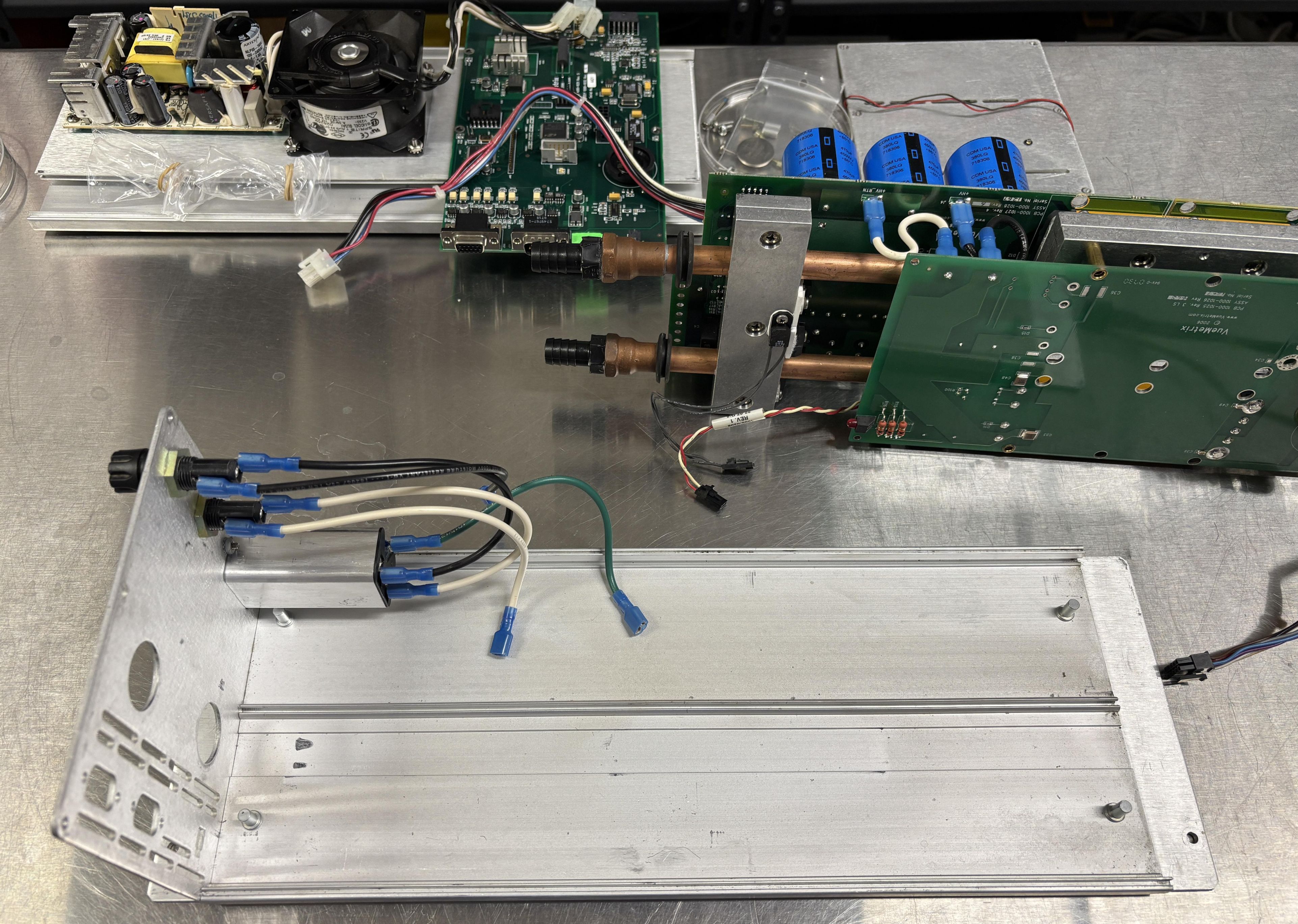
Once the rear aluminum plate is removed, and the AC input section connections are disconnected. The entire board stack, heatsink, and water cooling lines can be removed as one unit. The water connections are loosely held in place with rubber grommets, making this removable without having to remove the end fittings or hose barbs.
Once the board stack is removed, we are left with a partial aluminum frame, the fuses, and the AC line filter/input socket. One of the PCBs rests against the channel in the center of the bottom aluminum plate.
DC-DC Converter Board Analysis
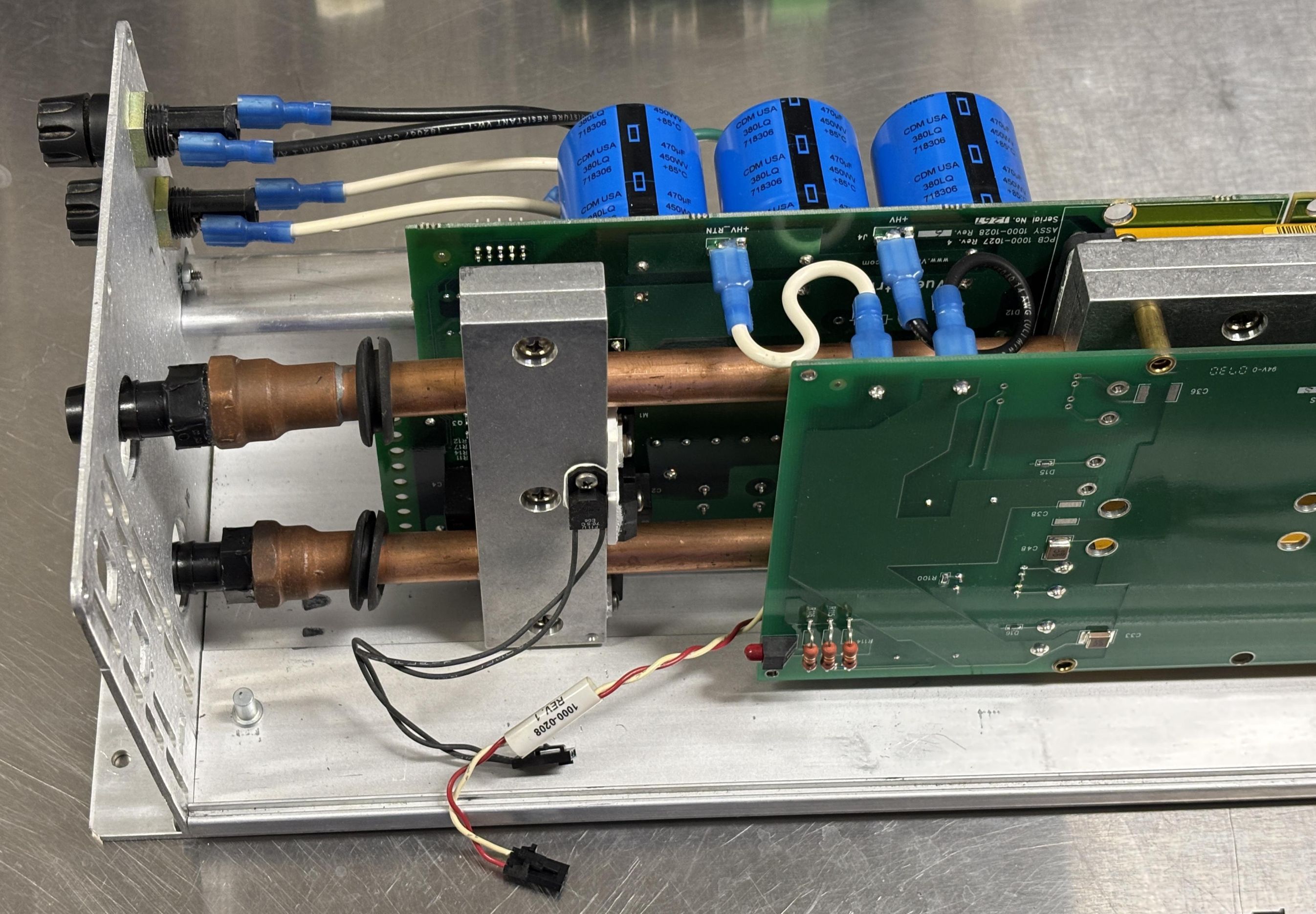
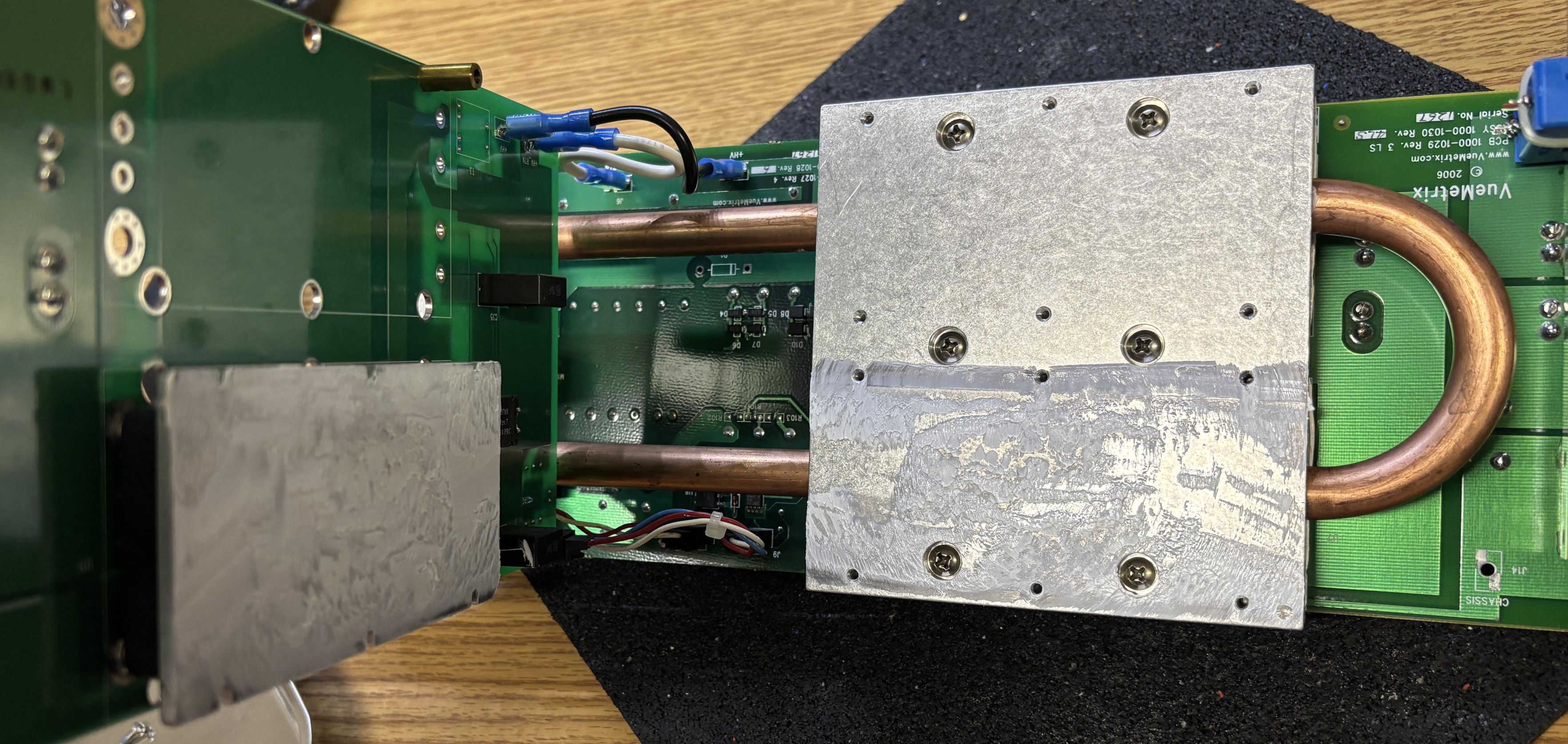
This is the primary DC-DC converter board which also contains the PFC circuit and rectifier. It has 2 DC-DC converter modules, which are secured to the heatsink and water cooling lines. The rectifier and some input-switching section components are also mounted to the heatsink. The part number for this board is 1000-1027.
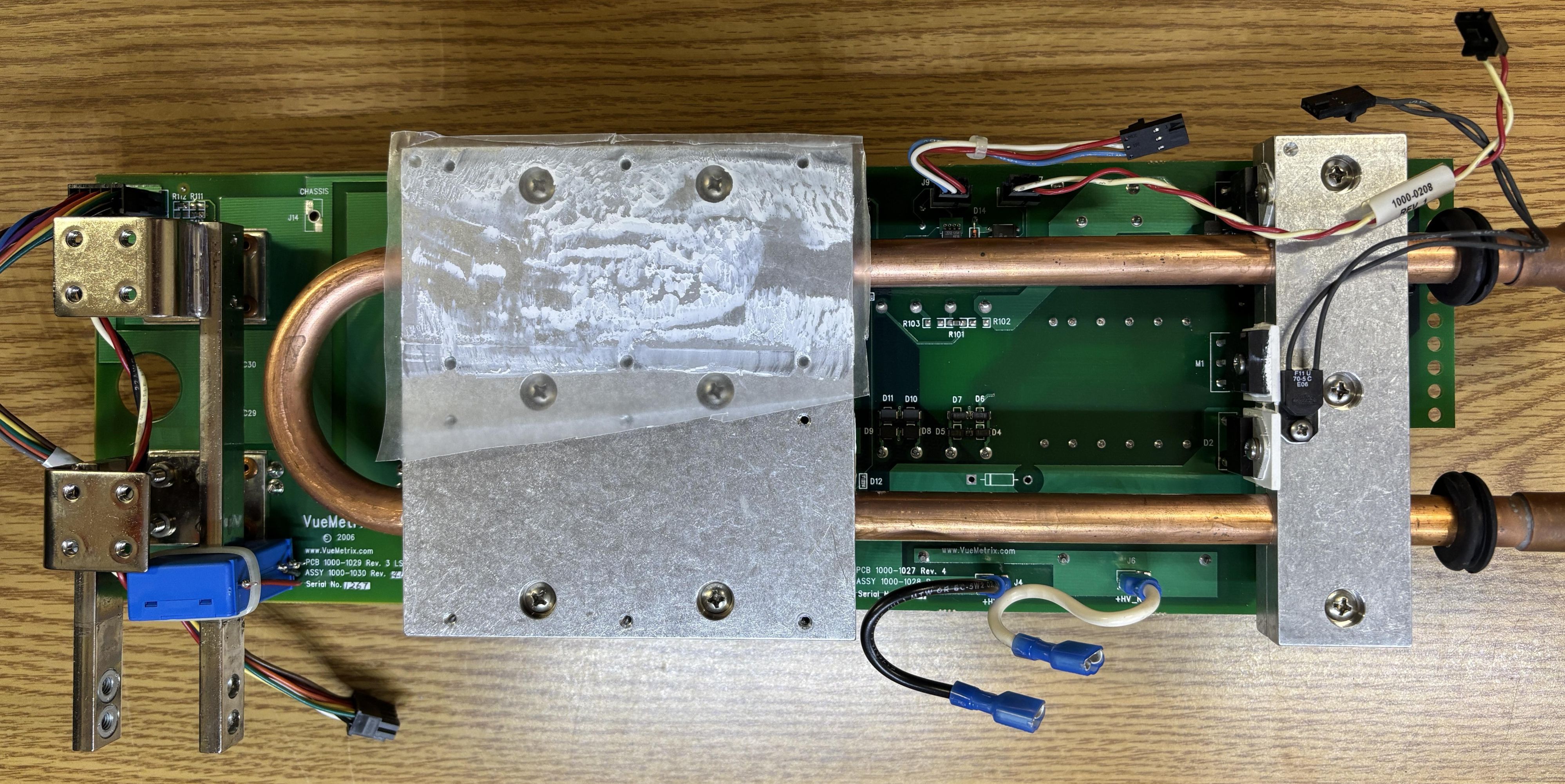
The secondary DC-DC converter board is also bonded to the same heatsink assembly. Either board can be removed by undoing the screws that hold the DC-DC converter module(s) against the heatsink assembly. The PCBs have holes that allow a screwdriver to access the Philips screws that secure the modules to the heatsink.
In the image below, the secondary DC-DC converter board is being removed from the heatsink assembly while the main DC-DC converter board is still attached. A copious about of thermal compound is used between the converters and heatsink to ensure adequate thermal transfer.
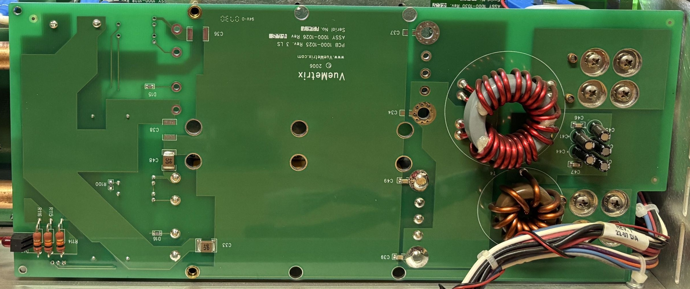
This is the secondary DC-DC converter board, which is populated with only one DC-DC converter module, but has provisions for two. The module on this board is wired in parallel to the converters on the other board in order to increase the system's capacity. This board receives high-voltage DC input from the primary board's rectifier section. The output of the DC-DC converter is directly coupled to the busbars and studs in the same way as the primary DC-DC board. Lastly, this board has one 3-pin connector for the DC-DC converter module parallel connection and primary control input. The part number for this board is 1000-1025.
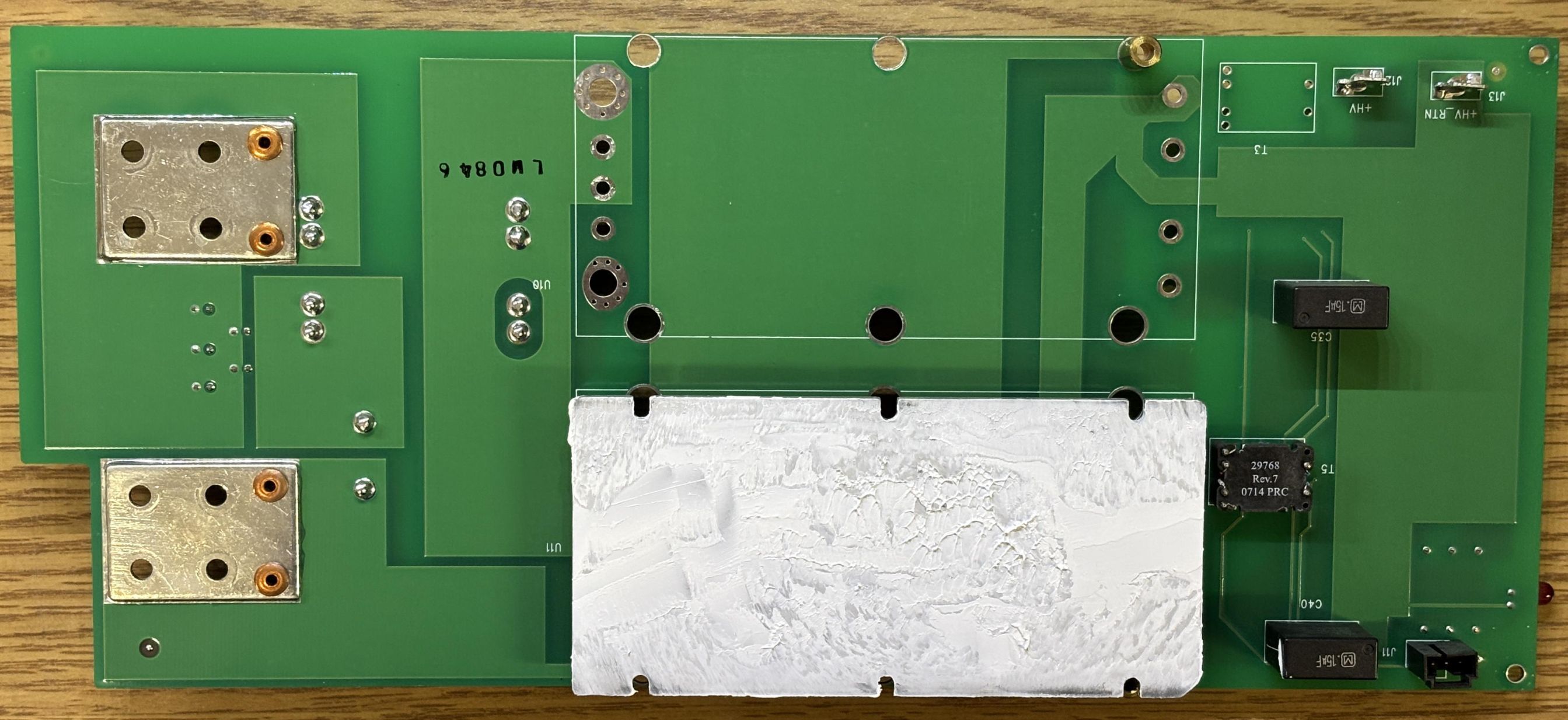
On the other side of the secondary board are two contact plates (left side) that are secured to the laser diode busbars to carry the high current DC power. In the center is the module itself, and on the top right are two spade lug terminals for the high voltage DC input (from the primary board). The small 3-pin connector on the bottom right is for a short jumper that connects the DC-DC converter PR and PC pins to the units on the primary board.
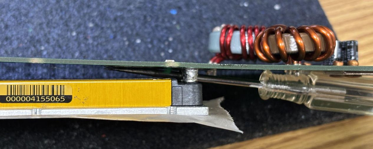
Desoldering the DC-DC converter was an absolute nightmare. The pins/studs are so large that it's challenging to dump enough heat into them to fully melt the solder. Additionally, some are coupled to the metal side of the module which acts as a heatsink, dumping all that heat. Using a combination of a soldering iron, heat gun, and screwdrivers to pry the pins out on either side as they were heated, we eventually removed the module. The reason we put so much effort into removing the DC-DC converter was to determine the make and model, as this would be instrumental in getting this diode driver working. Dealing with the CANBUS and anti-tamper nonsense that AMS implemented in the digital control board was likely going to be much more difficult than driving the DC-DC converters directly. Putting the module back was was much easier. We used solder wick to remove the solder from the holes in the PCB, re-installed the module, and soldered it into place.
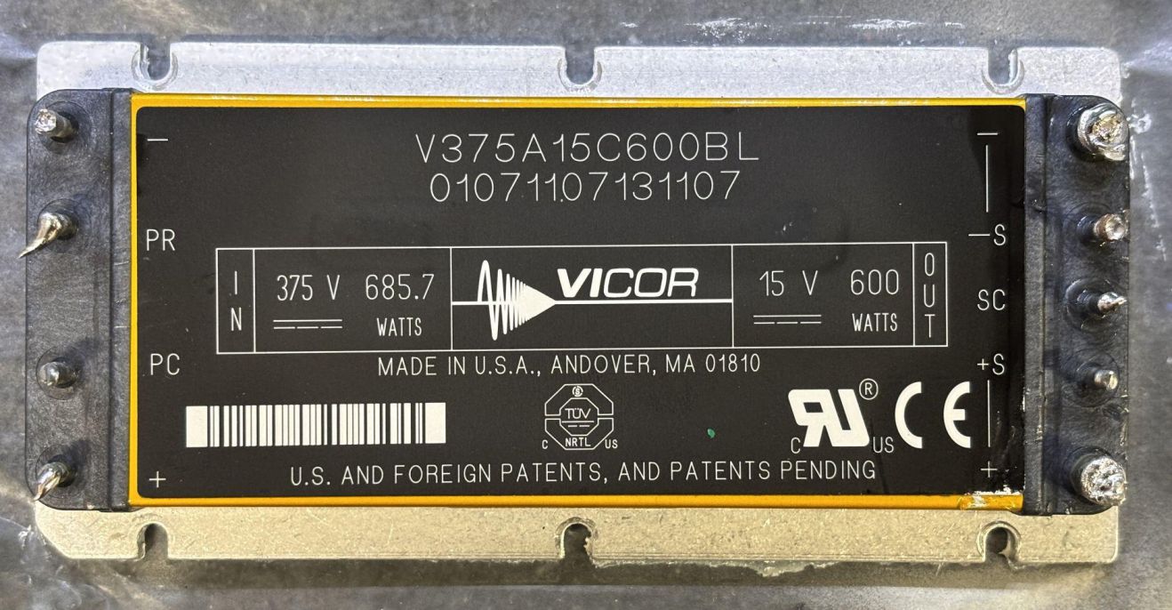
At last, the fruits of our labor! As far as we can tell, there is no documented disassembly of these VueMetrix Vue-HV diode drivers. We wanted to get to the core of what was actually driving the diode stack. It turned out to be quite simple: three Vicor V375A15C600BL DC-DC converter modules wired in parallel to achieve the desired output current. This is not a cheap part, they retail for around $800 on DigiKey and are very efficient and reliable units. They are marketed to industries such as medical and aerospace.
Seizing the Means of (power) Production
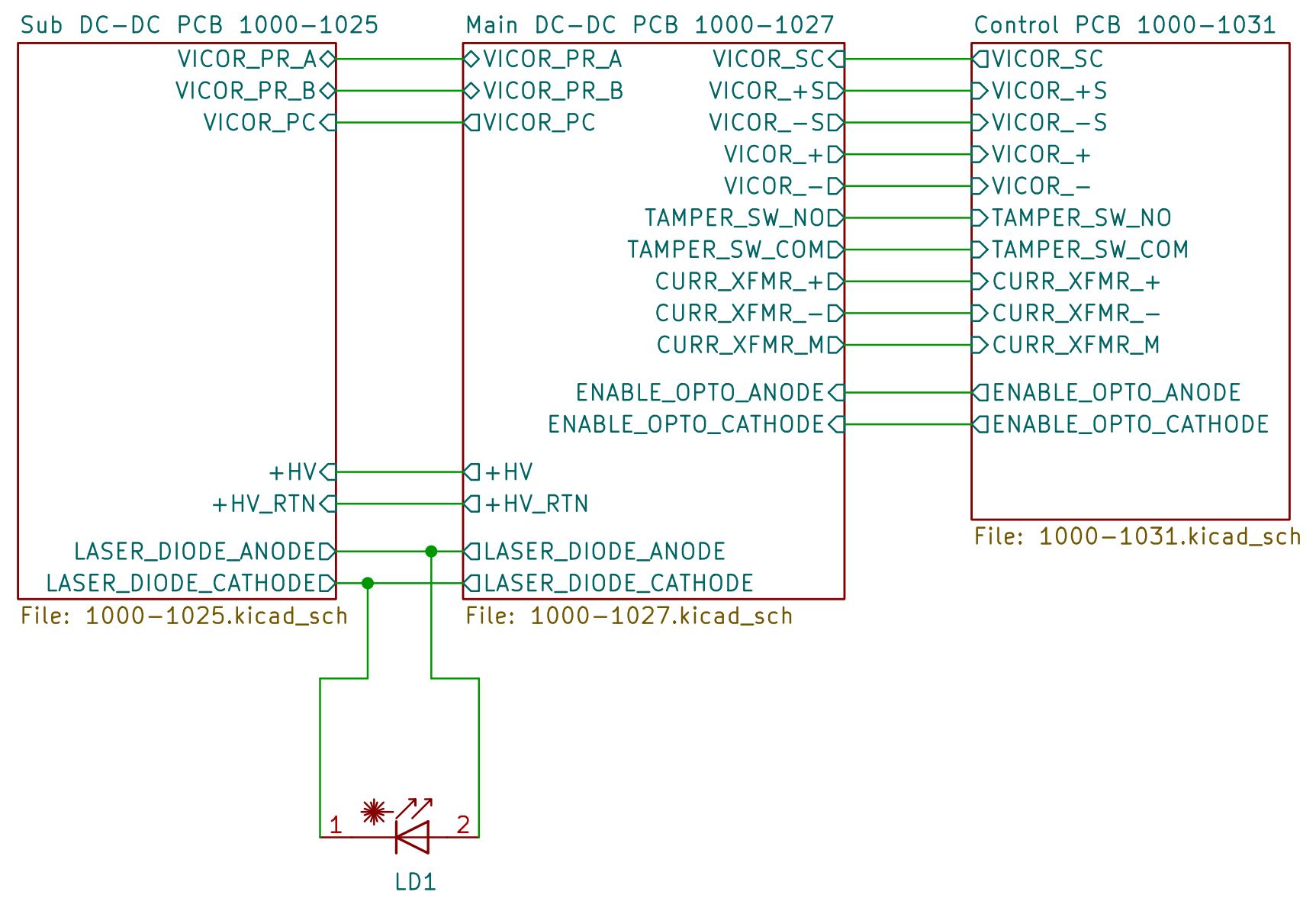
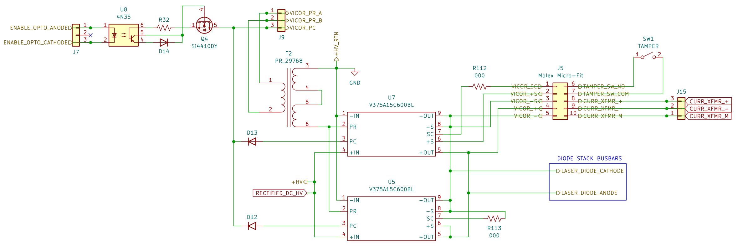
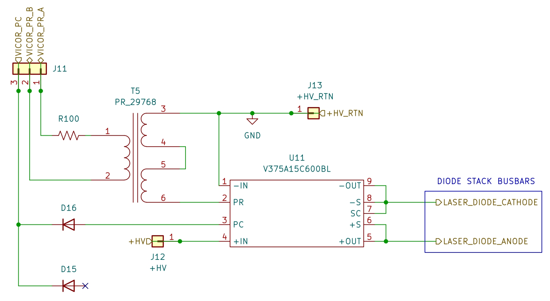
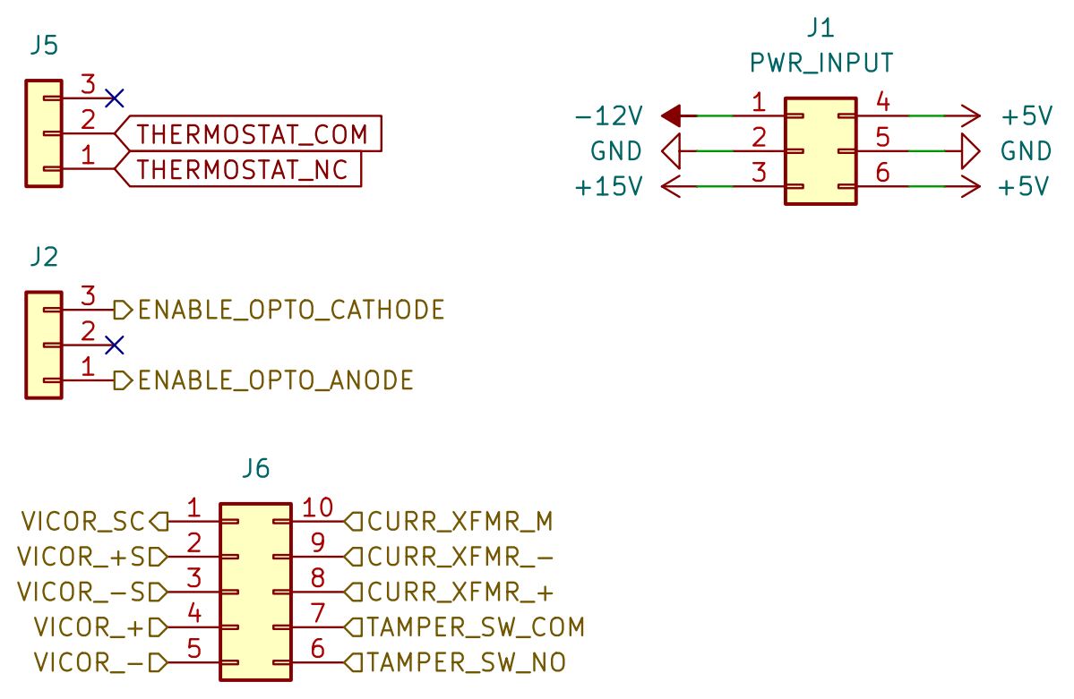
We spent significant time reverse-engineering the DC-DC boards to understand exactly how the Vicor modules were wired up and being controlled. Luckily, this turned out to be straightforward. The three Vicor modules are wired in parallel, with the inputs as well as the outputs paralleled together, across the two boards. The PR (parallel) pin of the Vicor modules is used to allow them to communicate and share the load in a parallel arrangement. Small isolation transformers (Vicor PR 29768) are used in between them for protection and interference reduction. The PC (primary control) pins of each module are all tied together with a diode in front of each module to protect it. The PC connection routes to J7 on the primary PCB. It also gets passed through J9 to J11 on the secondary PCB containing only one DC-DC module. PC is only used to disable the modules, it cannot be used to adjust the voltage. The PR connection is also passed over from the primary PCB to the secondary PCB through those connectors. Output voltage adjustment or trimming is done via the SC (secondary control) pin and S+/S- pins on just one Vicor module (U7) on the primary PCB. S+ and S- are used for accurate output voltage sensing and will avoid voltage drop since they are dedicated sense connections separate from the actual power delivery pins. Adjusting or "trimming" the output voltage is clearly outlined in Vicor's documentation. A resistor, potentiometer, or voltage DAC can be used to trim the voltage up or down by changing the resistance value between the SC and +S pin (trim up) or -S pin (trim down). More resistance = more trim (greater voltage difference from the nominal output). These particular modules have a nominal output voltage of 15V, so leaving the SC pin floating causes them to output a clean 15V DC. Since the other modules are connected via the parallel communication pin, they have SC tied to ground and S+ and S- tied to the positive and negative outputs, respectively. The other modules act as slaves and follow the output voltage trim of the master module (U7). The schematic below identifies the connections between the three boards within the VueMetrix diode driver. Understanding these connections is critical to bypassing the digital control board and driving the Vicor DC-DC converters directly. We are currently developing a custom board that is intended to be a drop-in replacement for the AMS digital control board. This page will be updated once that project is complete.
This schematic represents the control section of the primary DC-DC converter board (1000-1027). Importantly, the schematic only includes the DC-DC converters and related control logic. The PFC circuit, rectifier, and ancillary components have been omitted as they are not relevant for this exercise.
This schematic represents the control section of the secondary DC-DC converter board (1000-1025). This board is essentially acting as a slave to the primary board, as it only has three connections for control, two for parallel to the other Vicor modules, and one for primary control (enable). Other than that, the Vicor module's output is tied directly to the diode stack busbars and it receives high voltage power through two connections that route directly to the primary converter board.
Lastly, this schematic is a small excerpt from the AMS digital control board (1000-1031). It is just to identify the connections that lead to the other boards. Since our plan was to bypass this board entirely, we didn't waste time fully reverse-engineering it. This board performs the following critical functions: Vicor module enable, Vicor module secondary control (output voltage trim), heatsink thermostat monitoring, current transducer monitoring, and output voltage monitoring.
WARNING: The steps below explain how to enable the DC-DC converters and trim the output voltage. These drivers are designed to drive some very powerful laser diodes. Be aware of what you have connected to the output. If your driver is connected to such a laser diode, or something else dangerous, double-check everything and be careful before enabling the output. This driver will effortlessly sink over 100 amps at the nominal output voltage and does not believe in second chances. This is your last warning.
- 1. Remove the AMS digital control board and apply 240V AC power to the Vue-HV diode driver.
- 2. Use a resistor, potentiometer, or voltage DAC to trim the output voltage up or down to the desired value. Vicor has an online calculator for this and the formulas are listed in their applications manual. For example, if the module's nominal output voltage is 15V and you want to trim down to 12V, you could use a 4,000 ohm resistor between SC and -S (pins 1 and 3 of the J5 Molex Micro-Fit connector on the primary DC-DC converter board).
- 3. Apply a small voltage (1.2V - 1.5V DC) to pin 1 of the J7 connector on the primary DC-DC converter board, and use pin 3 of the same connector as ground. That will activate the emitter of a 4N53 phototransistor optocoupler and enable the Vicor modules (primary control). The modules should now be outputting DC voltage.
- 4. Remove power from the J7 connector (Vicor module primary control) to disable the output.
As a test, we used this diode driver to power the Coherent FAP800 pump diode within a New Wave Research Jasper HP laser head. We trimmed the voltage down to around 2.5V and it worked great!
Check out the datasheet for the Vicor module below along with the applications manual which includes pictures of the inside of the module. Vicor is a pretty awesome company for actually including pictures of the inside of their product along with detailed descriptions that explain how they work. A PDF version of the schematics shown above is available for download below. These schematics were developed by us during our analysis of this system. No public schematics exist for Vue-HV controllers.